KOKUSAI ELECTRIC has the world's largest share in batch deposition equipment and single wafer treatment equipment, which are highly regarded by semiconductor device manufacturers around the world.
Semiconductors now have a history of over 70 years. In that time, its evolution and diffusion have dramatically changed industries and our everyday lives. And leading the forefront of this evolution is KOKUSAI ELECTRIC. We are founded on a long history, cultivating our know-how of semiconductors. In 2018, we became an independent specialty manufacturer of semiconductor manufacturing equipment. Among the many processes of semiconductor manufacturing, the KOKUSAI ELECTRIC Group is developing its business mainly for the deposition process, which influences semiconductor performance. In October 2023, the company was listed on the Tokyo Stock Exchange Prime Market in anticipation of future growth.
In recent years, the structure of semiconductors has become more sophisticated and more three-dimensional, and decreasing productivity and increasing difficulty in the deposition process are the most important issues for semiconductor device manufacturers. The wafer surface has become more complicated in shape, where an enormous number of narrow and deep holes and grooves are formed. This expands the surface area requiring deposition. In addition, the travel distance of gas required for deposition has become longer, increasing the time required for deposition. This reduces productivity and increases the necessity of deposition with a high degree of difficulty. Solutions to these problems are batch ALD technology and treatment (film property improvement) technology, both of which are our strengths.
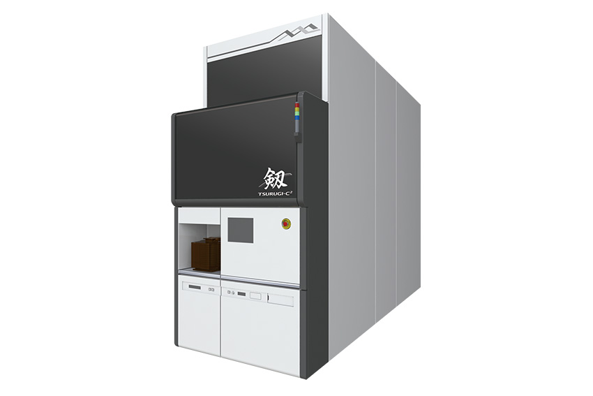
Batch ALD* technology that can achieve highly difficult deposition and high productivity at the same time
The single-wafer equipment forms wafers one by one, whereas the batch equipment can form 50 to 200 sheets of wafers at a time, which is characterized by high productivity. The ALD technology is a high-difficulty technology capable of producing high-quality thin films with good step coverage, and its demand has been increasing along with the evolution of semiconductor devices. This technology had a problem with productivity because gas is supplied cyclically so it takes time for deposition. However, combining the ALD technology and batch technology has allowed us to achieve high-difficulty deposition and high productivity at the same time. Our batch ALD technology can be said to be the most logical solution that responds to the evolution of semiconductors.
Our deposition equipment adopting batch ALD technology is highly regarded by semiconductor manufacturers around the world in the 3D NAND field, where the semiconductor device structure has already become sophisticated and three-dimensional. The demand for our technologies and expertise accumulated for 3D NAND will also expand significantly in the fields of DRAM and Logic, which are increasingly becoming more sophisticated and three-dimensional.
* the KOKUSAI ELECTRIC Group refer to a technique for thin-film deposition at an atomic layer level involving a process of cyclical supply of multiple gases as “ALD.”
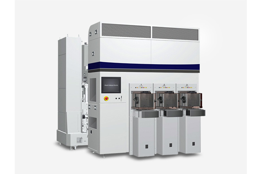
Treatment (film property improvement) technology with superior isotropy and step coverage
Treatment technology is a technology that provides treatment (film property improvement) in a broad range of temperatures by plasma and heating after the deposition process.
Our single-wafer treatment equipment is a solution that achieves film property improvement with superior isotropy and step coverage and with high productivity through abundant radicals produced by our unique plasma method. With the deposition process tending to become colder, the demand for film property improvement using plasma has been increasing, and our equipment has already been adopted in the fields of NAND and DRAM. The adoption of Logic will be the next turning point.
Ultra-high temperature activation annealing equipment designed for the SiC power device market, which is expected to grow further
In recent years, the demand for systems for SiC power devices has been rapidly increasing. An ultra-high temperature activation annealing equipment taking advantage of our technology is also being developed. We expect that its mass production will become a further turning point and accelerate the growth of systems for SiC power devices.
Future business development
In anticipation of the expansion of data centers and investment to reduce environmental load (GX: Green Transformation), the semiconductor device market is expected to grow significantly in the longer term, with the semiconductor structure continuing to become more sophisticated and three-dimensional. Our corporate slogan is “Technology & Tai-wa for Tomorrow.” We will identify customers’ essential needs through “Tai-wa*” and create innovation through “technology” accumulated over many years, thereby offering solutions to customers.
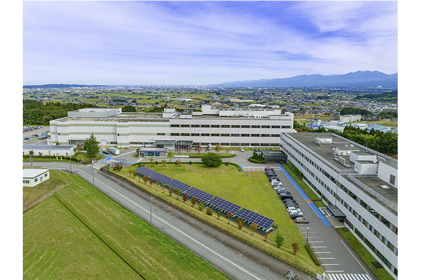
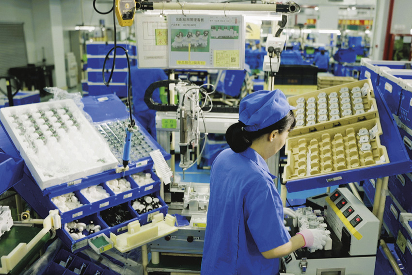
Produced in Toyama Prefecture, Japan and South Korea (Photo: Products and Toyama Technology & Manufacturing Center)
In accordance with the KOKUSAI ELECTRIC Way, a new management concept we formulated as a company engaged in the evolution of semiconductors, we will pursue value from the perspective of both business activities and ESG efforts and contribute to the achievement of SDGs while aiming to simultaneously achieve the realization of a sustainable society and sustainable development of our group.
*Tai-wa is a Japanese word meaning dialogue or conversation between people face-to-face to be willing to understand others with a sense of empathy. At times, subjects we have Tai-wa with can be things besides people. For us, Tai-wa implies respecting every one of you, being sincere, and acting wholeheartedly, that is ‘an attitude itself towards work’. This is our group’s DNA that we value to have last forever.


0 COMMENTS