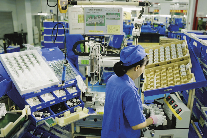
Since 1972, Ueno Seiki has been a reputed manufacturer of visual inspection equipment for semiconductor and electronic components, holding a top share in this niche market.
Japanese monozukuri is famous for its attention to detail and the kaizen philosophy has become known throughout the world. Quality, cost, and delivery (QCD) have become essential for modern-day businesses. Your company has been around for over 50 years and specializes in inspection equipment for semiconductors, a very niche field. Can you tell us more about your monozukuri and the advantages it brings to your business, especially as you operate internationally?
Our corporate philosophy is “creating value,” and if we were to put things simply I think that is what we are doing every day. We are thoroughly committed to providing a solution-based business, and we are always striving to utilize our technology and our products to resolve the challenges and problems our clients might be facing. What we are looking to do is not necessarily aim to be number one in the market, rather we are looking to have the best solutions and the best technologies in certain categories, so that is essentially where our focus lies. Not to chase profits, but rather to be the best for customers. An example might be with being the one with the loading power control for damage-free handling or visual inspection technology that makes visible micro defects that are difficult to detect. Even from the beginning, we are looking for those niche areas and leading in those areas. I think that has been the key to our growth and we as a company have prided ourselves on our ability to provide solution-based services.
In the 1980s and 1990s, Japan was the undisputed leader when it came to semiconductor manufacturing thanks to its dominance in memory products such as RAM. In the 2000s we saw a switch in the market over to TSMC foundry-style production, which was ideal for large-scale integrations such as microprocessors. Japan then went into a decline, and although the country has seen a drop in terms of fabrication capacity, Japan still has a market share of 30% for global semiconductor manufacturing equipment and 40% for semiconductor manufacturing-related materials. What is your analysis of this evolution and what do you think is the role of the Japanese industry in today’s semiconductor supply chain?
I think it is just as you have said, and Japan still leads the way when it comes to the actual equipment that is used for manufacturing semiconductors. Additionally, you have the materials. I think the reason Japanese firms have maintained dominance in these fields is because of our supreme fine-tuning and optimization with different kinds of technology and craftsmanship. This is best characterized by the Japanese word suriawase, and I think this is really where we and other companies can show our strength to the world. Ueno Seiki can really shine in this department, especially when it comes to inspection equipment.
Many commentators have suggested that the Japanese monozukuri is under threat with its declining population. Already 29% of Japanese citizens are over the age of 65 and it is expected that Japan’s population will plunge under 100 million by as early as 2050. How is your business reacting to these population changes and what steps have you put in place to prevent them from becoming bigger issues further down the line?
First and foremost, as a company, we are looking to increase the recruitment of international employees and additionally, we are looking to expand our global staff as we look to continue the globalization of our company. I actually believe that this kind of challenging circumstance is a great opportunity for us as well, and when we as people get too comfortable we forget to push ourselves and think outside the box. As the situation is so tough it has pushed our company to grab ripe opportunities as soon as they present themselves.
Another very important aspect is that this situation has put us in a place where we need to strengthen our HR policies as well as the education and training that we can provide for our staff here at the office. When you get fresh graduates through you need to strengthen them to become talented engineers, and practical training is indispensable in that respect. We are looking to provide that kind of training and accumulation of skills for our foreign workers as well as our Japanese.
What is your take on the Japanese ecosystem as a hotbed for semiconductor production once again? With new fabrication plants opening up all across the world, how will you cater to foreign demand overseas?
We definitely cannot ignore the geopolitical impact the semiconductor field plays globally. In order to ensure a stable supply chain of semiconductors, you see that there are a lot of huge moves when it comes to countries backing their industries. One of the reasons TSMC chose to work in Japan was because the Japanese showed their commitment by providing that sort of investment.
Regarding the geopolitical aspect including the need for various countries to create economic security assurance policies, I think that is what was behind the push you saw and the investments and incentives provided by the related countries. In any case, if there is a market where our technology can be utilized, it is our role to establish a system to support our customers in that market, and we will continue to work on this.
Your company is known for creating the world’s fastest semiconductor inspection devices, sorting good semiconductors from bad ones. Could you give us a little insight into the key technical milestones in your company’s history over the past 50 years that have brought you to the company we see today?
One thing that is overlooked in our company’s history is the fact that we were dealing in discrete handling system technology when the whole market was still moving in the direction of large-scale integration (LSI) and memory. LSIs and memories require long test times for complex testing, and our technology to transport a single chip at high speed cannot demonstrate its value. Discrete semiconductors, on the other hand, require very short test times and are produced in huge numbers, so our high speed technology creates great value.
In the semiconductor testing world, there are the handlers and the testers, and in the LSI market the handlers are relatively cheap, but the testers are expensive. When you're talking about discrete semiconductors, however, things are reversed and testers are very affordable whereas the handlers are more expensive.
In this sense, we believed that the market would recognize our value in testing for discrete semiconductors, especially in high-speed handlers, because faster handlers can increase productivity.
Back in those days when LSI was the standard and the boom led the market in that direction and oftentimes I would be asked why I didn’t provide testing for that. I would tell those who asked that it isn’t where our technology can shine, and it just didn’t make sense to enter the LSI market when our technology could make a much bigger impact when it comes to discrete devices. We are always strategically looking to see where our technology could shine the most. That is why we believed that we were able to show our strength when it came to electronic components, not only in semiconductors but semiconductors and surrounding components.
Filters are an example and you can see that electronic components these days are continuing to grow and evolve at an even faster speed than semiconductors themselves. When it comes to that phase and that level you can see that our technology is still able to compete and thrive.
When we interviewed Torex Corporation one of the things that surprised us was the size of the devices; sometimes you can barely see it on your finger. Miniaturization comes down to being able to pack as many transistors as possible onto as small a surface as possible. How do you keep up with the miniaturization trend that is sweeping the semiconductor industry?
I think the key is always speed, and so far today we have only talked about discrete devices, but as a whole, our competitive advantage that we can leverage is the fact that we can provide inspection at really high speeds so that companies and clients can enhance their productivity rate while also maintaining a certain level of functionality. As the trend pushes the industry towards more compact and thinner chips, what is important is to be able to control loading power and still provide the solid external visual inspection that is required. All of those things can be done at slower speeds, and if you slow down the speed you can do anything inspection-wise, and that is ok if you are talking about the research phases, but when it comes to production, speed becomes one of the most important factors. This is where we are looking to make sure that we can enhance the speed at which we can inspect.
I like to think of it as an egg. If I handle the egg and inspect it very slowly the egg should be fine, however, if I handle it very quickly the chances of damaging it increase. Semiconductors and similar devices are the same as an egg in that sense. They are complicated and are getting smaller and smaller. Our competitive technology allows us to inspect these devices at speed with no damage, leaving the device completely damage free. Basically, we provide high-speed, high-precision inspection services to our clients.
I think this is overlooked often, and at times very misunderstood. There is an importance to doing such high levels of inspection because it lowers the total cost involved. By reducing the required number of machines you can cut your operating costs, running costs, and even energy consumption costs. It can even go to save space within the fabrication plant itself.


One product that encompasses all of this is the LT-evo, perhaps one of your most famous products. It is designed for ultra-small devices and features a six-sided vision inspection system, laser marking ability, and a patented Z-axis power loading system. What motivated the launch of this particular product and what clientele are benefiting the most from this LT-evo machine?
Last year, a leading telecommunications device company asked Ueno Seiki to supply its inspection equipment for an important device used in one of the latest product models. As a result of our high-speed visual inspection equipment, they were able to minimize the amount of inspection equipment needed for inspecting on 1-micron level defects. It is important to understand how expensive these devices are, and we were able to help the customer cut down on used space in the plant as well as electric power consumption and inside running costs. I think this is a fine example of what our company can offer.
Just recently there was an electronics exhibition that caters to device manufacturers, the exhibition is called Nepcon, and there we were able to announce new equipment called the LT-neo. This LT-neo can operate at speeds of 120,000 units-per-hour (UPH) which is lightning fast when compared to the already speedy LT-evo that operates at 70,000 UPH. We also announced the RS-neo, which is follow-up equipment to the RS-evo.
With our product lineup, we have four major models, the LT, RS, RP and WS lines. LT is an integrated test handler which has integrated testing, laser marking, and six-sided visual inspection features. The other lineup comprises the RS, RP and WS lines. This lineup incorporates features for visual inspection. The big differences between the four lines are the product inputs, which for RS, RP, WS are wafers and LT has some other input methods.
In response to the question of what motivated this development and product launch, I think it comes down to our confidence; we truly believe that we are the top makers in the field. We want to be the ones that are pushing the outer limits of what is possible and leading the evolution of inspection devices. That is why we are looking to continue to give birth to new generations of products and in that way, continue to dominate. Following our company slogan, we are always looking for the “next one;” the next challenge or opportunity. This is something that company-wide we are fully committed to.
For years demand in the semiconductor field came from electronic components, but nowadays we are seeing a plethora of new applications and devices such as 5G smartphones, all the way to the metaverse and VR devices. Looking to the future, what applications do you think will be the next vector for growth in the semiconductor field?
I think it will continue to be the communications field, and IoT is the same way. Right now our largest market is communications and I think acceleration in technology advances will continue in this field with the progress of new technology such as 5G and 6G. We want to make sure that we are thoroughly involved and penetrate this market, especially when you consider the processing speeds required within that industry. I believe our inspection levels match up and we can provide the equipment that meets the speed and precision needed by these manufacturers. I think additionally it is the same when it comes to cars, and they are also a form of communication technology. More and more the automotive sector is incorporating cutting-edge technologies and sensors, and that sort of inspection is a strong suit of our company. For example, I believe the next generation self-driving car has hundreds of sensors. With our visual inspection equipment, we could be indispensable in that respect. Those sensors and LiDAR technology are where our inspection technology shines.
When you talk about the automotive sector, cars themselves nowadays are essentially computers on wheels. They operate similarly to smartphones and other communication devices.
We’ve talked about hardware today, but equally important is the software. Your company has its own proprietary UNICON software which is using AI-based detection systems to find micro-cracks in components. Can you give us an insight into how you developed this system? How do you train this AI software?
UNICON is our proprietary visual inspection software. This system is constantly evolving by incorporating not only general-purpose visual inspection functions, but also our own know-how and algorithms gained from the new challenges and cases we have experienced. In addition, since technology advances rapidly in this field, we regularly upgrade the software based on the latest technologies and findings. One of the challenges in visual inspection is overkill, in which what is originally a good product is judged as defective. It is very wasteful to discard expensive good devices as defective. Human power is still needed to make the final judgment of good or bad, but if this could be automated, it would have a great effect. We are also examining the potential for various applications of AI, which has been the focus of much attention recently; the field of application of AI is very broad, and we expect that there is great potential for differentiating our products. We are also collaborating with universities and outside research institutions on joint projects in these areas.
Since 2001 you have been present in Shanghai, and since you have expanded to Singapore, Taiwan, Hong Kong, and Malaysia. Can you tell us a little more about why you selected those locations? Moving forward, are there any new regions or countries that you are targeting for future expansion?
From a manufacturing perspective, the Kitakyushu area has been known as an industrial place where the first steel furnace was built in Japan. Actually, local people have inherited a manufacturing temperament, and take pride in their monozukuri culture.
In terms of the market, it just comes down to having a market there. There are markets that need our technology, so it is logical for us to chase that. We have already established our support base in North America, but there are other possibilities, for example, in Europe, if there is a market there. In Asia, one possibility would be India, which is expected to grow.
Imagine that we come back and interview you again on the last day of your presidency. What goals or dreams do you hope to achieve by the time you pass the company on to the next generation of Ueno Seiki executives?
The first issue I’m always thinking about as president is ways to be able to respond to the needs of our clients and meet their expectations. Secondly, I want to ensure that our employees prosper and are happy. Thirdly, I want to be able to provide solid succession and growth to the company. These three issues are always first and foremost in my mind, and sometimes I think that 90% of my brain power is expended by these three areas.


0 COMMENTS