Toray Research Center (TRC) isn’t your average lab—it’s a high-tech, solutions-driven powerhouse leading the charge in materials analysis and innovation across a vast array of industries.
Could you start by giving us a quick introduction to the Toray Research Center and the kind of research projects you undertake?
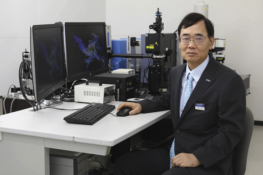
First of all, I would like to briefly introduce my background. I joined Toray Industries, Inc. in 1986 and was assigned to the Toray Research Center, Inc. (TRC) immediately after joining the company. From May to October 1998, I studied at the Fraunhofer Institute in Germany. My main research field is the structural analysis of gallium nitride. Following the adoption of my project by the New Energy and Industrial Technology Development Organization (NEDO) as a project leader in 2003, I was subsequently selected as a project sub-leader by the Japan Science and Technology Agency (JST). This enabled us to secure funding for the development of cathodoluminescence and Raman spectroscopy equipment, as well as synchrotron radiation-based near-field infrared spectroscopy equipment. During the five years from April 2010 to March 2015, I participated in the R&D Partnership for Future Power Electronics Technology (FUPET), a project focused on new material power semiconductors for realizing a low-carbon society, and served as the leader within the TRC. I was also recognized as a Fellow by the TRC. In September 2010, I received the Advanced Analytical Technology Award - JAIMA Instrument Development Award from the Japan Society for Analytical Chemistry, presented by Chairman Atsushi Horiba of HORIBA, Ltd.
In April 2014, I was appointed as the leader within the TRC for the NEDO project on new material power semiconductors for realizing a low-carbon society. In 2020, I was awarded the title of Senior Research Fellow by the TRC. I also served as the leader within the TRC for the NEDO and METI project on international standardization for SiC epitaxial wafers. In June 2023, I was appointed the president of the TRC.
Personally, I have authored around 70 academic papers and 13 books and have filed for six patents. On March 24, 2023, Springer published my culminating work on my research at the TRC, titled “Advanced Optical Spectroscopy Techniques for Semiconductors.”
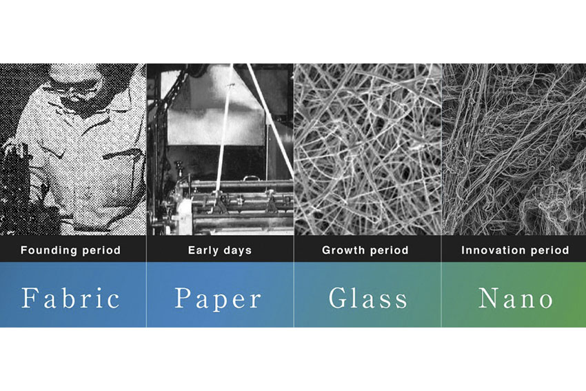
Now, let me explain a bit about the TRC. The TRC was established in 1978 as a company providing contract analysis services, separate from Toray's research division. It is a wholly owned subsidiary of Toray. At the time of its establishment (FY1979), it had 69 employees and sales of 750 million yen, 65% of which came from direct business with Toray. As of last year (FY2023), the number of employees had grown to 515, and sales had reached 9.5 billion yen, with only 9% coming from direct business with Toray. In other words, recently, 91% of its sales have come from business with companies other than Toray. Since its establishment, the TRC's fundamental philosophy has been “Contributing to society through advanced technologies.” The motto of our business operations is "Technology" and "Trust."
We have more than 2,000 clients, including companies and research institutions both inside and outside Japan. We receive requests for solutions to various issues related to research and technological development, production troubles and complaints, patent disputes, and R&D trends. The TRC's business model is to provide problem-solving analysis support services. Through close communication with our clients, we propose solutions and build trust. We serve various industries, including semiconductors, displays, IT equipment, life sciences, and batteries. Analyses related to semiconductors, batteries, and materials—our main fields—are conducted at our laboratory in Shiga Prefecture, while analyses for pharmaceuticals and biotechnology are carried out in Nagoya and Kamakura. We have three sales offices in Japan: Tokyo, Nagoya, and Shiga.
In 2018, we established our first overseas subsidiary in Shanghai, and in October of the same year, we set up an analysis center at the Toray Automotive Center Europe (AMCEU). We have a sales agent in Korea and a sales representative stationed in Taiwan.
For 46 years since our founding, we have continuously introduced and developed cutting-edge analytical technologies to differentiate ourselves from our competitors. At the same time, we have worked on developing pre-treatment, measurement, and analysis techniques to drive business expansion.
Next, I will briefly discuss the role of the TRC in semiconductor analysis. Not only do we introduce the latest analytical instruments, but we also develop our own devices in line with global trends. With a wide range of analytical instruments capable of analyzing semiconductor materials from both nano and macro perspectives, we are at the forefront of semiconductor analysis. We focus on understanding the overall landscape of the semiconductor industry and solving potential challenges that may be encountered during production. Our uniqueness is demonstrated through the extensive range of analytical instruments we have access to and our own proprietary analytical devices. We constantly collaborate with academic institutions, writing papers and presenting our findings at international conferences. By showcasing our technology, we aim to contribute to technological innovations. In particular, our state-of-the-art electron microscopes offer high spatial resolution and analytical capabilities at low acceleration voltages.
I participated in all national projects for power semiconductor development across three different phases. In the first phase, from 2010 to 2014, I focused on defect evaluation of SiC wafers. In the second phase of NEDO's SiC project, the TRC was responsible for analyzing power devices and material degradation. The third project, which concluded last year, focused on semiconductor standardization. SiC power semiconductors are a new type of power semiconductor that can replace Si power semiconductors. However, their drawback is that they degrade quickly due to the high power they require. It was found that as the operating current level increases, defects (TED: Threading Edge Dislocation) begin to form and grow from the surface to the interior. This research was awarded the Young Scientist Presentation Award by the Japan Society of Applied Physics. Not only does this study contribute to the development of new types of SiC power semiconductors, but it also deepens our comprehensive understanding of defect formation and growth. In addition, we have successfully observed the local stress distribution in SiC devices by using a near-field Raman spectrometer developed in-house. While planar-type SiC devices have been common, the increasing availability of cost-effective trench-type transistors has led to further advancements in high withstand voltage, high integration, and miniaturization, resulting in the development of new types of trench-type SiC power semiconductor devices. As miniaturization progresses, transistor defects have become a significant issue. To enhance the performance of these trench-type SiC transistors, many of our customers have expressed a need to verify whether the trench structures are being formed as designed. Our near-field Raman spectrometer has revealed stress concentrations localized within a region on the order of a few hundred nanometers at the trench tip. Furthermore, the TRC is the only company in the world that utilizes NanoSIMS for analysis.
NanoSIMS boasts a minimum beam diameter of 50 nanometers and a detection limit at the ppb level, with an analyzable depth ranging from a few nanometers to several hundred nanometers. While this technology has been used mainly in geoscience, geology, biology, and materials science, the TRC has applied it to the semiconductor industry and life sciences.
In semiconductor composition analysis, STEM-EDX is the standard method, but it does not have sufficient sensitivity to detect impurities. However, NanoSIMS, with its high detection sensitivity, can detect low concentrations of boron, aluminum, and phosphorus in devices. This technology has been well received by customers who require high accuracy and sensitivity. In November 2022, we introduced a world-class electron microscope with cutting-edge performance. A unique feature of this electron microscope is its placement within a custom-designed enclosure, providing exceptional vibration and noise resistance. Equipped with two aberration-corrected electron lenses—one for the condensing system and the other for the observation system—it allows for more precise and higher-resolution observations. While the spatial resolution of conventional electron microscopes was 86 picometers, this state-of-the-art microscope achieves a spatial resolution of 53 picometers. It is also possible to set different electron beam acceleration voltages for each measurement sample. With our advanced microscope, it is possible to observe surface damage within a nanometer.
In September last year, we introduced a new analytical device called the Hydra Multi-Ionic Plasma Focused Ion-Beam (FIB), which is used for front-end semiconductor processing. To prepare samples for observation under an electron microscope, technology to process them into a thin layer of around 100 nanometers is required. Interestingly, our new FIB processing device can not only operate 40 times faster than conventional FIB devices but also process larger areas. It can utilize four different gases—xenon, nitrogen, argon, and oxygen—to process samples. The device can handle sizes of several hundred micrometers in width and over one millimeter in depth, with an accuracy of tens of nanometers. It allows for the creation and processing of larger observation targets at higher speeds, enhancing efficiency and enabling versatile observations.
Now, let’s take a look at our future plans for semiconductor analysis. Our business strategy is to swiftly introduce the latest analytical instruments and develop pre-processing, measurement, and analysis techniques as early as possible. By doing so, we can lead the analytical industry as a pioneer in the analysis business.


We all understand that the semiconductor industry is in constant evolution. While in the past smartphones drove change, now we are seeing generative AI and semiconductors for the automotive sector drive some of the change. Each application requires different materials and different approaches. As a research company, how do you ensure that your employees are always up-to-date when it comes to providing the best solutions for your customers? How are you able to position yourselves at the forefront when it comes to the semiconductor industry knowing that constant change is in the DNA of industry as a whole?
First, let me share my personal perspective. When I joined the TRC, I initially started out researching diamonds. After that, I studied abroad at the Fraunhofer Institute for research on GaN. Just a week before my arrival, Professor Akasaki, a Nobel laureate, was conducting research in the same room. I have been involved in NEDO’s SiC power semiconductor project from the beginning, and in the latest project, I actively participated in the development of power semiconductors using SiC, GaN, and Ga2O3. On the other hand, diamonds are a material I have been researching for over 37 years. This pioneering spirit has been passed down not only to the TRC but also to me personally.
Global demand for semiconductors is surging, and the tension between the U.S. and China is further driving this need. Currently, Japan and the U.S. are working to strengthen their domestic production capacities to meet the growing demand. As a company, it is crucial to constantly upgrade ourselves and maintain our position at the forefront of the industry. We achieve this by introducing the latest technology into our analytical instruments and developing our own unique techniques and methodologies.
As the president, I aim to make the TRC a true research center, not just an analysis company. My vision is to make the TRC not only a company that contributes to Japanese society but also a globally recognized company with cutting-edge analytical technologies. It's been 37 years since I joined the TRC, and I aspire to build a solid foundation that will ensure the company continues to grow even after I retire. Since a company is made by its people, nurturing our employees is key to achieving this vision. What I want to convey to our employees is to never fear failure, maintain a spirit that embraces challenges, and continue to pursue the development of new technologies with unwavering determination.
One of the biggest issues facing the semiconductor industry is sustainability, especially when it comes to water saving and energy consumption. How is your company enabling your customers to become more sustainable and achieve their sustainability targets?
The TRC is working to replace materials with those that have lower carbon footprints as an initiative across the Toray Group. We are also considering introducing material recycling technologies, including chemical recycling. Analyzing the differences in impurities between virgin materials and recycled materials is important to understand the optimal use of recycled materials.
Another area of your expertise is battery analysis, which addresses the challenges associated with capacity, durability, and safety. You offer customers composition, deterioration, and performance analysis. Within that deterioration analysis, what are some of the primary indicators that you look for to assess changes in the composition and structure of active material surfaces?
It is unavoidable for batteries to deteriorate in some way. Chemical reactions cause discharges, which disintegrate the anode and cathode. We focus on ions using an electron microscope and observe changes in the surface of elemental ions. We also measure the discharge characteristics and the impedance generated. The impedance changes with the number of battery cycles, and this data can be used to determine the level of degradation.
In other interviews we have conducted we have often heard the importance of partnerships to unlock overseas markets or to co-develop new and exciting products. What role do partnerships play in your business model and are you currently looking for any new partnerships either domestically or overseas?
We collaborate with specific academic institutions and equipment manufacturers, and this co-creation practice is crucial for developing analytical devices. By having unique devices, we can gain pioneering advantages over other companies in the industry. We are constantly seeking new collaborations with domestic and international partners who can enhance our technology.
We conduct joint research with international companies and universities. For example, we have exchange programs with engineers and researchers from a university in Germany. This means we are always at the forefront of research and development in the analytical industry.
We know that your company is not just focused on Japan, having a worldwide presence in countries such as China, Korea, Germany, Taiwan, and many others. Are you interested in continuing this international expansion to other regions and markets? If so, where are you targeting next?
We are currently strategizing for international business expansion. Our main target for semiconductors is North America, but we are also focusing on Southeast Asian countries, such as Singapore and India. For the battery business, our targets are Western countries, particularly the United States. In April 2023, we established the Energy Storage Device Division by integrating our research and sales teams. This allows us to comprehensively analyze batteries both domestically and internationally.
Amid the rising tensions between the U.S. and China, many countries are now attempting to nationalize battery production. Europe and the United States are at the forefront of this movement, making these regions key targets for our business strategy.
As someone who has been involved in semiconductors for many decades now, how do you envision the next ten years for the semiconductor industry here in Japan?
The 20th century is called the age of oil, and the 21st century is rapidly becoming the age of semiconductors. The demand for semiconductors is particularly growing in new fields, such as generative AI, bioscience, and electric vehicles. As for materials, I believe that diamonds will be the most crucial in the future. As I mentioned earlier, when I joined this company 37 years ago, my first mission was to research diamonds as a potential material for semiconductors. I confirmed the efficiency and effectiveness of using diamonds as a semiconductor material.
I confirmed the efficiency and effectiveness of using diamonds as a semiconductor material. Tensions between the U.S. and China are expected to rise in the future. As a result, the competition over semiconductor development will intensify, particularly between China and the United States. When it comes to flash memory, I actually think South Korea will take the lead. Japan's position in this industry is a significant concern. Currently, Japan's strength lies in power semiconductors, with companies like ROHM, Toshiba, Mitsubishi Electric, and Fuji Electric at the forefront. I believe it is important to focus on our strengths rather than chasing market segments like memory devices. We need to pool our respective strengths to create a national project that will shape Japan's future.
For more information, visit: www.toray-research.co.jp/en


0 COMMENTS