In the current landscape, Japanese manufacturers face the challenge of navigating supply chain diversification prompted by policies like the US Inflation Reduction Act (IRA). However, Japan’s reputation for reliability and advanced technology positions its products favorably. Additionally, the weakened yen leaves Japanese made products more cost-effective and appealing globally. How can Japanese manufacturers strategically leverage the current conditions to enhance their competitive advantage?
It is important to diversify risk by establishing a diversified supply chain. This will increase resilience to geopolitical risks and policy changes. For example, regarding the US sanctions on Chinese semiconductors, we can mitigate risk and promote business continuity planning (BCP) by transferring manufacturing from China to Japan for products destined for the US market. This is more feasible with a weak yen.
Competitiveness is not simply a matter of price competitiveness but also encompasses factors such as quality, delivery time, BCP, and risk mitigation in the supply chain. Still, thanks to the weak yen, Japanese products can now be offered at more competitive prices, so it is important to seize this opportunity to enter new markets and expand market share in existing ones.
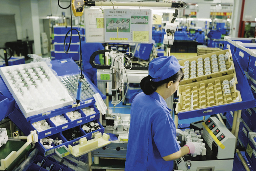
Japan is facing a demographic decline, with the oldest population in the world and one which is decreasing each year. This is creating staffing shortages and production bottlenecks, with Japan forecast to confront a deficit of over 11 million workers by 2040. This means Japanese companies will find it difficult to hire staff while also facing a declining domestic market. How is your company reacting to these challenges, and to what extent must Japanese companies look overseas to secure new markets and talent?
Our company is focusing on enhancing the skills of existing employees and introducing automation technologies and robotics. This will help ease labor shortages and production issues while improving efficiency.
In anticipation of the declining Japanese domestic market, we are actively pursuing entry into overseas markets. This will provide a new source of revenue and foster the company’s growth.
When we think of factories, the image that often comes to mind is dominated by men. However, looking ahead, we are considering placing more women in factory settings and hiring retirees to address labor shortages. We also expect that new ideas will emerge from the perspective and rich experience of women and more experienced workers.
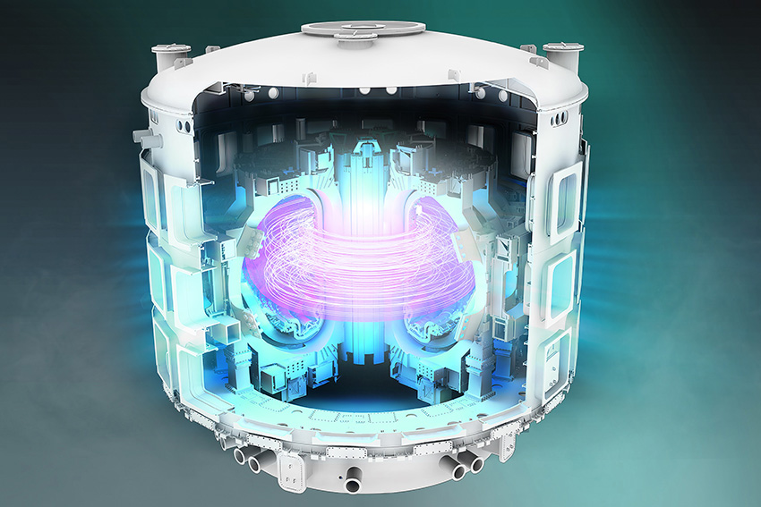
As enterprises attempt to diversify their production bases, Western industry leaders are increasingly viewing Japan as an alternative production and research hub. On top of IBM’s collaboration with Rapidus, Japan has attracted investments from major foundries. These include TSMC’s new fab in Kyushu, as well as investments from Micron Technology and Western Digital, among others. Many industry experts consider Japan’s advanced ecosystem in semiconductor materials and equipment to be a strategic advantage to bringing production onshore. What do you think are the comparative advantages of Japan as a production and research hub, and how do you expect the onshoring of chip production to affect your business?
Japan was once the world leader in semiconductor manufacturing. The supply chains and material manufacturing technologies established during that time still exist today. We believe that this serves as motivation for wanting to establish semiconductor production bases in Japan. Our company currently operates four factories and five sales offices domestically, and we believe we have an advantage in our ability to provide meticulous service.
A significant trend in the manufacturing sector is the increased integration of technology. When we spoke with the president of Sodick, he had an interesting take on the four key elements for precision parts manufacturing: you need the latest and most advanced machinery, advanced CAD/CAM software, a controlled production environment, and the best raw materials. With such a setup, we see a decreasing need for workers because IoT and Big Data are now integrated into the manufacturing process to oversee all four stages. In such an automated and controlled environment, what role will engineers play in the future of the sector?
The field of engineering is constantly evolving. Our daily lives today are vastly different from those of twenty years ago, and this change trend will likely continue. In this context, it’s important to adapt to those changes. Therefore, the ability to adapt becomes crucial. Engineers will not only have to instigate change but also consider how to adapt to these changes for the benefit of the company and the public.
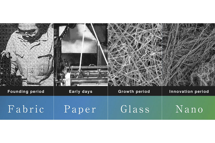
Your company was founded in 1976, and since then, it has expanded to the field of quartz glass products for the semiconductor industry and established a presence in China and the United States. What do you consider to be the milestones in your company’s history?
Some of the major milestones are entering the semiconductor sector, going public, expanding and investing in China, and transitioning into a holdings structure.
Your cleaning process can be applied to a wide variety of materials, such as ceramics, silicon, and metals. However, it faces the challenge of avoiding damaging the base materials. Maintaining the integrity of the original surface while achieving thorough film removal is crucial, especially for coated products used in high-precision applications. What are the key parameters and conditions for each cleaning method you offer to ensure minimal damage to the base materials, and how does the cleaning process handle complex geometries and delicate features on the parts being cleaned?
Clean particles are critical in our production, so maintaining a clean production environment is the key. Conventionally, we have used an air particle detector to determine how many particles are emitted from production and feed this data back to the cleaning device, but now we have developed and introduced a liquid particle counter. This device is embedded in water to count the number of particles that are emitted through processing, and we still use that data to give feedback to the cleansing device.
Another unique technology we use is diffusion bonding. It enables to create interior channel pattern inside Quartz and encapsulate any other substrates. Also we can embed a code so customers can scan it to get the needed information. We have a patent on that. It’s like a QR code embedded within quartz glass, so it won’t extrude and cause any extra particles.
We also do dry cleaning using a dry ice blast. This new method applies dry ice to chill and contract the quartz, and then we heat it again to expand it. By continuously going through this contraction and expansion process, we can remove the surface particles. To ensure quality, we leverage AI for the inspection instead of relying on the human eye, so we have higher accuracy in finding defects. In fact, there are so many possibilities for using AI to increase quality and replace people, so we would like to incorporate these technological capabilities actively.
In the semiconductor industry, cleanliness will always be a pressing need for an industry that works with exact components. The trend, of course, is miniaturization, with the number of transistors on a chip doubling every two years, as famously predicted years ago and known as Moore’s Law. New technologies are also coming to the market. For example, ASML from the Netherlands is introducing its EUV lithography systems, which haven’t yet taken hold in the industry but are expected to. In terms of your product development, could you give us an insight into some of the new products you’re working on or new R&D you’ve been doing and how you’re keeping pace with developments in the industry?
The difference I need to reiterate is our business model. We are not a research and development-oriented company. Rather, we are a commissioned manufacturer of components for semiconductor equipment maker developed. Our role is to provide the required components quickly, efficiently, and with low pricing, so our capability lies more in production. Whenever we receive a new model or request, our engineers work with our client’s engineers to find the best form or solution for the purpose and production. So, catering to a major manufacturer’s needs quickly, efficiently, and with low pricing are the three keys to our business.
Having said that, our research and development is focused on how to enhance the productivity and efficiency of the production. For example, particle emission is the most damaging to semiconductor production, so we have developed and introduced both hot and cold methods and automation to avoid as much human contact as possible. We have also introduced an automated liquid-borne particle counter (LPC) cleaning method. Coating is the key to increasing surface capacity, so we do surface treatment using chemical vapor deposition (CVD) and a double-layer spray service. For example, that could be applied to a semiconductor machinery tube that lets gas go through. We also promote using a type of material that would mitigate the chance of having dust particles on the surface and, as already mentioned, we introduced a dry ice cleaning method. Those are some of the approaches that we have been taking.
You completed a series of distribution agreements with GE Quartz in America in the 1990s and, more recently, with a Chinese company. Are you currently looking to partner with any other companies for distribution or to enhance your productivity or R&D efforts?
We have extensive partnerships with our suppliers. For example, with our material suppliers, we have a yearly contract for the materials that we need for manufacturing.
Currently, our focus is shifting more towards partnerships with maintenance service providers. We want to create a global network of local partners who can manage maintenance when needed. For example, for our maintenance bases in the US and Korea, we would be the ones to train the partners that we work with, and we would ensure the quality, but our partner companies would do the actual maintenance. We would like to expand this network throughout the globe. Quartz is a high-end product with a higher pricing range, so rather than transporting it back to Japan, it is better to have a local base for logistics and cost reduction reasons.
You now have three production bases in China. Do you see any new locations that you will be expanding to in the coming years, and in terms of the business, where do you foresee the most growth opportunity for the semiconductor industry?
With the China-US dispute about semiconductors, our production policy has been greatly impacted. Previously, we were centered on our Chinese base, and we first sent the products made there to Japan and then distributed them from Japan throughout the world. Because of that, it’s important that we strengthen our production capacity in Japan so we can export the products produced here to the global market and use the Chinese factory to produce mainly for the Chinese market. I believe the economy will strengthen at the end of this year or next year for sure, so if we start a new factory overseas, it would be taking more time Instead, moving earlier within Japan and focusing on opening up new markets. And from a market point of view, the US, primarily Arizona, is our biggest target.
As a company about to celebrate its 50th anniversary in two years, let’s imagine that we will interview you again then. What would you like to accomplish over those next two years as a company?
There will be a new company structure. On May 10, we announced a plan to have a new holding company called GLTechno Holdings, which will combine the two companies. It should take effect on October 1st, once we receive approval from our shareholders in June, so that will be our new structure.
Our relationship with GL Sciences will no longer be a parent-child relationship. It will be a group company with equal standing, so that will be a huge benefit for us. GL Sciences has a long history with more employees, and its R&D team has over 100 employees. Their focus is analytics, which is not necessarily semiconductor-related. Still, we will be able to leverage their human resources, expertise, and finances to start new businesses or make new developments, so we want to take advantage of the synergy. In two years, when we have our 50th anniversary, we will be operating as a new company, so it would be nice if you could come back and interview us again, and we will then be able to showcase our new strategy to you.


0 COMMENTS