As pioneers in advanced technology solutions, Tamagawa Denki leads the way, from precision plastics, cutting-edge semiconductor design, and AI-driven automation.
Today is a pivotal time for Japanese manufacturers with policies such as the US Inflation Reduction Act that is forcing corporations to diversify their supply chains for reliability reasons and to reduce country risks from countries such as China. Japan is known for its reliability and advanced technology, and with a weakened yen, “made in Japan” has never been more cost-effective and trusted on an international scale. However, Japan has also faced stiff price competition from neighboring countries such as China and Korea. What are the advantages of Japanese suppliers in this current market environment and how do you navigate this price competition from nearby countries such as China?
Originally, we have been working in the domestic market, and with our medical clients, we produce domestically and then provide and ship products domestically. When our customers are more price-focused, of course, they may turn to Chinese manufacturers, but if our clients are dealing with domestic customers as well, then they tend to choose our products, which are of high quality. So if the customer is only price-focused, then I think we cannot win in that.
I would like to ask you more of a demographic question because, in the next 15 years, one in three people will be over the age of 60. This can lead to a labor shortage and a shrinking domestic market, but it could also pose opportunities such as increased production of automation technologies. For Tamagawa Denki in particular, what are some challenges and opportunities that this demographic shift has caused and how are you reacting to these?
Of course, from a long-term perspective, this declining population in Japan is an issue. However, looking at the regions, not looking at central Japan, there are very smart engineers around the regions and districts, so if we can provide engineering resources to these clever people, I think they will deliver a good performance.
Regarding the aging society, we think that not only for the semiconductor industries but for all industries, this will become a significant opportunity. At Tamagawa Denki, we are trying to create an environment so that engineers can work for a longer period of time, and from a business aspect, we believe that new devices will be developed in the future. For example, regarding agriculture, we believe that many services that would enable workers or farmers to work more easily will be developed in the future.
It’s interesting that you mentioned new devices are going to be developed because in today’s ever-evolving market of electronics in semiconductors with new technologies such as AI, 5G, and cloud computing on the rise, by 2028, the global electronics market is set to hit over USD 2 billion, while the semiconductor industry is set to become a $1 trillion industry by 2030. As such, a comprehensive approach to analog and digital semiconductor design is crucial for delivering high-quality, efficient, and reliable solutions to your clients. How do you see the evolution of your company in the ever-growing industry of semiconductors over the next 12 months?
Regarding our semiconductor business and how it will develop in the coming 12 months, of course, we are also developing AI-related items, but these are really sort of cutting-edge devices. Looking at conventional components, I think we are expecting them to become more convenient, using IoT, so I think that is a likely future.
Interesting that you mentioned how you are also trying to do that physical part of it because your analog LSI design and evaluation division specializes in providing tailored solutions for analog technology, particularly focusing on power supply development and optimization. You offer a comprehensive approach that includes considering various aspects such as area, power consumption, and external component optimization. You also ensure a commitment to failsafe design principles. How do you determine the optimal selection for analog technologies given the project, considering factors such as power source compatibility and application-specific requirements?
Looking at the requirements regarding LSI for our customers, there is not much of an analog chip-only requirement. So, when we consider this analog power source, we have to consider what kind of movement we shall provide within which block, and with what timing. And based on that, we need to decide the specification or the power uses.
Looking at these analog components or parts, the size tends to be larger so we have to be creative about how to make it smaller. In order to do that, we have to carefully look at which block moves at what timing, so we will not deliver over-margin analog components. In this aspect, it is very important to carefully determine the size.
System on a Chip (SoC) is a very advanced process, and it requires a power device as well so it also becomes really important to control the leak in this digital block, so when you decide how to turn on or turn off the block, the timing of this power source becomes very important. Including all these aspects, it is very important to understand the specifications of the chip.
So, only analog is not all right, and digital-only is also not fine. We have to combine both analog and digital to determine the specification, and once the specification is decided, then we realize that.
It’s interesting that you mentioned digital because this also goes hand in hand with your digital semiconductor design offering, focusing on your RTL design, DFT design, layout design, and timing and physical verification. Could you discuss the strategies for maintaining efficiency and effectiveness in the face of technology trends and customer requirements in the realm of digital semiconductor design?
In the digital realm, the evolution of the tools is very quick, and in the software area, the evolution of the design tools is also very quick. Sometimes we find it quite difficult to fully use these ever-evolving tools and software. However, when it comes to really important, useful tools, the usual way is to realize effective and efficient design by customizing these very important tools. That is what we do.
In the digital area, we have many layers, starting from the front end to the middle end to the back end, so we can start from the very beginning until the very end. That is why we can use our know-how in customizing these kinds of tools.
Your company was founded in 1949. You started as a manufacturer of plastic components and parts, and now you’ve expanded into the LSI design business. As the president of this company, what would you say is the main competitiveness of your firm, and what makes you different from your competitors?
Our founder initially ventured into plastic molding before gaining independence from NEC. Until the financial crisis, particularly the Lehman shock, our primary focus was on servicing NEC. However, midway through, we diversified into semiconductor design as well. Historically, our collaboration was tightly knit with NEC, which later transformed into NEC Electronics and then Renesas. This early engagement with NEC, deeply rooted in the semiconductor industry, afforded us invaluable experience from the outset. We not only partnered in design but also delved into production methodologies. The educational support provided by larger corporations, during this period equipped us with insights into their operational dynamics. This comprehensive exposure enabled us to not only master design but also inherit crucial production expertise, thus solidifying our stature. Today, our strength stems from this holistic journey, where learning every aspect from development to mass production, under the guidance of an Integrated Device Manufacturer (IDM), has been a pivotal asset. This includes our learning from IDM, which has provided us with insights difficult to attain in the current mainstream horizontal division of labor.
We have strength and analog design, and when we do that, we work together with the customer. So, this process would be kept in mind with our customers and we are able to share the whole process with them. So, it’s not just delivering the data. When we work with Japanese major customers, they compliment us because we share our know-how and the whole process and this is very useful to them and that is how they evaluate us.
One of our strengths as a company is that we form a team, a combination of engineers, and by doing so, we are able to hand down know-how and technology to the next generation.
We have a code of conduct that we disseminate among all the employees. It is something quite natural, “Tamagawa-Quality”: Be honest, make reports documenting what you did, continue to improve (kaizen), and never give up. This sounds quite natural, but in the real world, it’s difficult to really implement these things, so we are very strict in following these items.
You mentioned, that you’ve been able to receive appraisals from Japanese major semiconductor companies. The semiconductor industry is set to become a USD 1 trillion industry, and, of course, Japan will play a major role. For example, TSMC is coming to Japan and Micron is establishing operations in Hiroshima. As a company that is supporting the semiconductor industry on top of supplying and providing services to the Japanese makers in that industry, are you also looking to diversify your customer portfolio and provide services to foreign companies, whether here in Japan or overseas?
Of course, if there is an opportunity to expand our business with overseas companies, we want to do that. And in our companies, we have a lot of engineers who have experience working together with venture capital, so if there is a good opportunity, we want to do that. However, we’re not thinking of simply outsourcing jobs, rather we are thinking of doing something together, working together.
We have been talking a lot about your LSI design business and I’d like to talk about your plastic precision division, which includes surface treatment methods such as organic solvent painting, water-based painting, and vapor deposition processing. This addition often has plastic, nonmetallic materials that are often like metal designs in terms of high-quality finishes. Can you explain the differences between this painting and its advantages, as well as what is the uniqueness of using vapor deposition over traditional painting methods?
Up to now, we haven’t made much difference with our competitors. However, in terms of Sustainable Development Goals (SDGs), we are trying to look for bioplastics and recycled plastics and we have another vapor deposition example (see photo below), with a very thin film. We are distributing these items at trade shows.
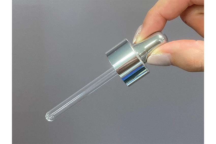

It looks like metal, but it’s soft. Actually, metal is applied, but it’s soft. It’s a non-linear sort of vapor deposition, using tin and indium. If you see this item with your eyes, it looks like solid metal covering the item, but when you use a microscope, it’s really fragmented so it does not crack and it is soft. Usually, when we try to do these things, it can easily peel off, but with our technology, it does not.
I have a last question for you, and this one is actually personal to you. Your company was founded in 1949, so you’re almost celebrating your 75th anniversary. Let’s imagine that we come back five years from now and have this interview again with you. What would you like to tell us? What are the dreams and goals that you would like to achieve? And if I can ask you a very difficult question, can you please define your company in one sentence?
What we want to do in five years is something we are now entering as a new business.
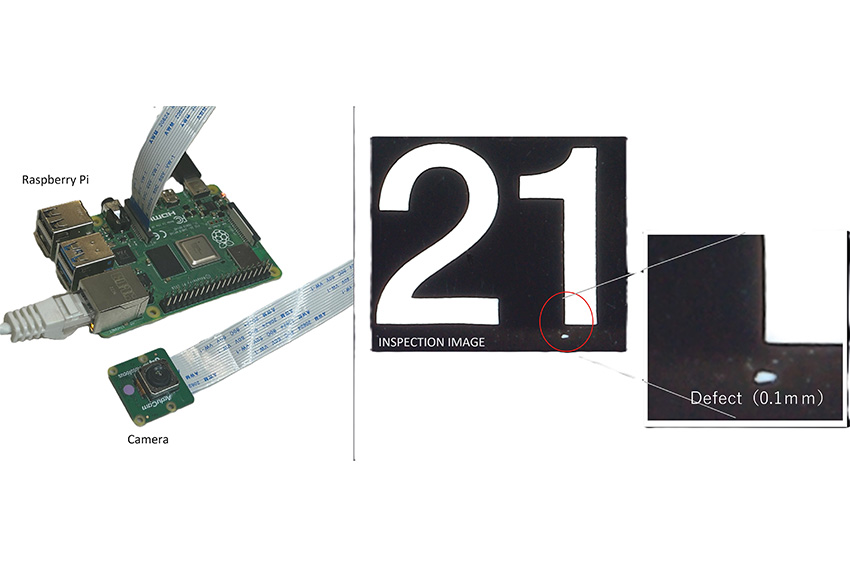
This very tiny little white spec (see photo above) is a bad point (size 0.1mm). This is defective. It has been identified by a machine, not by visual inspection. So currently we’re trying to do this and we are trying to automate the visual inspection of printed materials using a machine. We can detect this kind of tiny misprint.
This uses a Raspberry Pi and an ordinary camera. These are very affordable. Combining this with AI, we are able to create a sort of AI vision. Instead of using human eyes, we’re able to do the inspection in less time. So in five years, we want to achieve some good results in image identification and something to do with generative AI. If you rely on outside manufacturers, then it’s easy, but we cannot accumulate the knowledge or technology on our own, so we want to start from scratch internally. We started implementing or introducing this technology in our own line, and we are currently starting to operate with AI. In five years, I believe these technologies could further expand outside of the company as well, so looking at the regional areas of Japan, there are a lot of SMEs out there and they have difficulty purchasing expensive machinery, so when we can provide them with these kinds of technologies, then I think work would be more convenient and easier, and it will be possible to reduce the cost in these SMEs as well.


0 COMMENTS