Since 1947, Natsume Optics has continued its research and development of high-precision optics, laying the foundation for the world's most advanced optical technology.
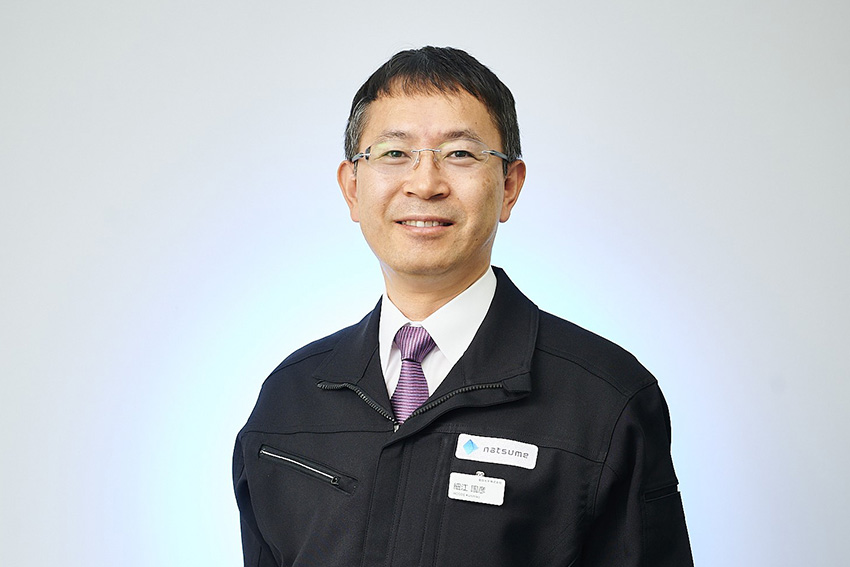
Mr. Hosoe Kunihiko, president of Natsume Optical, I believe you have prepared an introduction and presentation of your company today. Could you introduce Natsume Optics?
Our company was established back in 1947, so we are now in the 77th year since its establishment. Our headcount is 264, and our company has survived many hardships since we were established not long after the end of WWII. Today, we are holding this interview in our Technology Center, but in addition to this facility, we also have our headquarters in Nagano and sales offices in Tokyo. There are three satellites. Interestingly, in 2023, our location in Iida, Nagano was voted as the best place to live in Nagano prefecture, as well as the number one ranked rural area out of all rural locations in Japan. There are natural landscapes and wonderful views. In 2034, there are plans to build a Linear Chuo Shinkansen bullet train running from Tokyo to Iida.
Our main business focuses on the design, development, and manufacturing of precision optics. We stand at the crossroads of light and manufacturing technology, combining these elements to create our products. All 264 employees are dedicated to this end goal.
I would also like to highlight our company logo, which we introduced in 2023. The light beam penetrates, giving customers the impression of our logo. The company motto is “To make every step one towards the future.” This is something that the company has lived by for 77 years now, never wavering. Our value is to continue to take on challenges and never back down.
Company logo
You might be wondering why we use the word “challenge,” and that is because every step of the way is a challenge. If we put up our best efforts against any challenge, we can overcome any obstacle in our path. Our tool to overcome these obstacles is, of course, our light technology and manufacturing technology. This mindset really dictates everything we do here at Natsume Optical. I believe that based on our company philosophy, we have been able to achieve excellent financial results, and if you look back to the early 1990s, our company has grown around 4.2% every year. This is rare among Japanese companies due to the Lost Decades of the 1990s and early 2000s, and even during that period, we were successful. Think about some of the historical events that happened during that period. The Lehman Shock and the COVID-19 Shock are both examples of rough periods in which we were able to survive.
Our optics include near-infrared (NIR), which is 1,500 nanometers in wavelength, and X-rays, which are just 1 nanometer in wavelength. At the top of our list of products introduced are optics for the semiconductor industry. We also offer optics for flat panel displays, lithography, and even synchrotron light optics. This is all thanks to our high-precision technology.
Diversification is another core aspect of our company, and we try to avoid focusing on only one segment. To say the least, we are a one-of-a-kind company that captures a wide variety of optics for a multitude of use cases. There are four strengths that I would like to outline next. Our first strength is specialized optics, which are optics used for short wavelengths, from NIR and UV, to X-ray. Another strength is the wide variety of shapes we can provide. Not only do you have to have access to good raw materials, but you also have to base your technologies on grinding and polishing those various optical materials, another strong point of our company. We have specialized in this for many years, working hand-in-hand with customers to design products that they truly appreciate. I think one of the keys to the success we have had is through the opening of our Technology Center in 2005, as well as its expansion in 2016. I think I would be amiss if I didn’t mention R&D as well. The Technology Center went through a two-step process, with the first focused mainly on R&D in 2005, and the second happening with its expansion to include increased production in 2016. Throughout this entire process, the theme was always high-level precision. This center is equipped with top-notch equipment that allows us to produce optical optics. We preserve a special temperature here of 22 degrees Celsius. We also have a clean room environment in this Technology Center, which meets all worldwide standards. It allows us to inspect all optics thoroughly before they reach the production phase. Beyond that, nothing happens without the appropriate hardware.
The new era of optics that we are developing has come thanks to our partnerships and, in particular, our co-development with the University of Tokyo. We’ve also worked on academic approaches through core development research with the University of Tokyo, and that is vital due to the professors being the ones who lead the way in technological development. Good cooperation between academic and industrial partnerships is how to make advancements happen. Last year in April, we donated part of our finances to the University of Tokyo to open up a special lab, allowing for even more in-depth cooperation.
There are two reasons why we donated to this lab. The first is for highly precise optic development for X-ray purposes, which is an ever evolving product and seen through different kinds of perspectives in terms of utilization. The second reason is simply to foster human capital. Within this R&D center, we can motivate new engineers to devote a part of their lives to the development of new products or technologies, so building this environment alongside academic institutions can essentially create the next generation of pioneers. In fact, some of our employees have returned to receive their Ph.D’s from the University of Tokyo. We also have people working here who received their Ph.D’s from the University of Tokyo and made their way here to join our company. I might even go so far as to say that Natsume Optical and the University of Tokyo have a very special bond.
Another example of how academics have helped spread the word of Natsume Optical is when students and Ph.D. candidates attend symposiums or lectures and publish or announce their research at overseas universities. Of course, the theme throughout is ultra-high precision.
You have to remember that every optic has a different purpose. Things such as tolerance, shape, and size can all make a difference and add up when considering surface treatment. We can mechanically adjust the light so that we can direct it where we need it, depending on the application. In other words, surface treatment technology is crucial to further the utilization of optics. We are talking about ultra-high precision surface correction rather than just surface treatment.
To what do you attribute your success?
It has taken us 10 years to reach the introduction of our technology. We can vary the tolerance by as little as 0.1 nanometers, and this isn’t the limit. To have a surface correction tolerance of 0.1 nanometers or even 0.08 nanometers is something very special, and realistically there are only a handful of companies in the world that can achieve this right now. This is why it took 10 years to achieve our goal and finally introduce our technology to the world.
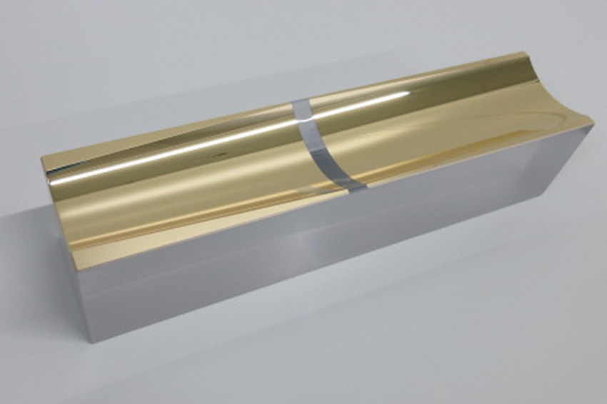
Wolter Mirror for X-ray
Next, I will introduce our X-ray optics, and X-rays themselves are something I would say the whole industry is focusing on right now. We are involved in a national project that is conducting cutting-edge research relating to X-ray mirrors. It demonstrates how serious the entire country of Japan is about developing new types of X-ray mirrors. X-rays can penetrate a cell, and you can analyze its structure or formation, even allowing for the detection of malfunctions within cells. I think it is very simple to understand because biotech is a very in-demand industry right now. Medical treatments, prototypes, and devices are very important to have before actual drug development happens. We’ve even had usage cases with imaging of hamster cells that can further the development of new medicines.
I’m trying to convey how vast the different applications and usages of optics are, so we try to come up with different solutions, shapes, sizes, and types. The use of our high-precision optics within X-ray devices actually brought media attention to our company. It was great to have the company’s achievements get media coverage.
Obviously, as a natural course, usage goes beyond biotech and medical, and recently, we have seen demand coming from the space exploration industry. NASA recently launched some rockets to study solar flares, and these rockets were equipped with X-ray mirrors, which were introduced by our company. They allow NASA to take X-ray shots of the sun to analyze, gaining better insight into the sun itself.
While our conventional business is lithography, which is used in the production of semiconductor equipment, we are trying to tackle a whole host of exciting and interesting industries to diversify our business further. Life science, medicine, and even space exploration are all targets.
We’ve always taken this standpoint where we look at what is on offer, and if it doesn’t exist in the world, we can research it, develop it, and produce it. This feeling has been present ever since our company was established, challenging ourselves to introduce new technologies and new know-how, and all of this inspiration comes from our founding fathers.
Our production rooms are all precisely temperature-controlled, and that allows us to be precise with our optics to the nearest percentage of a nanometer. The rooms are kept at 22 degrees to ensure the best conditions for grinding. Essentially, grinding is fiddling with the glass material itself, so that is why we need to have a special room with optimal conditions. All of this is fortunately automated, meaning that we can run our operations 24 hours a day, non-stop. Now you can understand why we need to control the temperature since day and night have different temperatures, and if an optic takes several days to grind, there are a lot of dips and flows in the external temperature. By controlling the temperature internally we are able to ensure that the best temperature can be preserved so that our machinery can produce the best results. High-precision manufacturing is something we are experts in, and it has always required an environment free of contaminants and external factors. Our Technology Center is on the outskirts, meaning there are no nearby roads. There are no intruders and no external factors, which is how we go above and beyond to preserve the special conditions we have established.
What would you say are the most difficult steps in your process?
I would say polishing is the most difficult. With our polishing machines, the glass is placed underneath, and a plastic material is applied as a mid-layer. It carefully polishes the surface of the glass. This room also requires special conditions. After the polishing is completed, we will check the surface of the glass, see if everything is up to specifications, and if not it goes back to the polishing machine again. It could be that optics go through the polishing step several times. Depending on the usage and the type of optics, we apply various different polishing machines. The methods of polishing also vary. It is important to have all these different polishing machines, so some of our equipment for polishing is created in-house.
We also have a special polishing room. Here, polishing is done using liquid slurry, and the room contains our most top-notch equipment. Having this special slurry on the surface allows us to be more precise in our polishing, which, in the end, results in more specialized optics.
After polishing is finished, the next step is measurement. Here, there are several types of machines that allow us to take precise measurements. This can be tricky since all optics have different shapes, sizes, and materials. They are irregular, so different kinds of measurement devices are needed. In fact, some measurements cannot be done by eye, so in those cases, we need to use special light measuring devices. All of our measurement devices are equipped with laser measurement. Interestingly, we make the optics for these devices, so we are making optics to measure our optics. Additionally, much of the equipment used in this step is produced in-house, and I think this speaks to a strong point of our company. Producing equipment in-house allows us to be a one-of-a-kind company.
What applications are you focusing on with all of these different pieces of in-house equipment?
Semiconductors continue to be our bread and butter, and show the most promise for the future. There are ups and downs across the industry, but we are now seeing the emergence of AI and robotics technologies, meaning there will be even more demand for semiconductors.
On our second floor is our clean room environment. Once optics pass through grinding, polishing, and measurement, special treatment needs to be applied to the surface in a clean room environment. This stage is referred to as the cleaning stage, but it is more like the finishing process. Inside the room is a water pool for the optics that will remove all pieces of dust, dirt, and other impurities. This is not the last stage, however, and coatings still need to be applied to the surface of the optics. You might think, “Why do you need to apply a coating?” First of all, this is for protection, but it also helps control light beams and reflections. The coating changes again, depending on the usage and the industry.
Inside the assembly room, people must wear special uniforms. This is where the final stage takes place, and all the final adjustments are made. When you have a PCB or something similar, the optics have to sit in the correct position; positioning is vitally important. During this assembly stage, we also apply a lot of technology and machinery.
With all of the in-house machinery you have that is automated, what role do you believe the engineers can play?
It is still very important to have wisdom behind us and the element of human touch. To some extent, we can entrust certain tasks to machines instead of human beings, but in some places, the wisdom of skilled engineers is irreplaceable. High precision may be marked by the technological upgrades we have in-house, but despite that, we still need to cross-check those improvements with a human touch. We have to check everything with our own eyes and make sure everything is safe.
You mentioned the human element, but overall, we know that Japan’s demographic situation is rapidly declining. It is becoming very difficult to find new engineers, which is creating a labor crisis and thus making this human element harder to fulfill. Can you elaborate more on how you are addressing this issue going forward?
Being a local company in a rural area means that we are struggling to attract new graduates to our business, but we are not alone, and the entire industry is having the same problems. We are at a crossroads right now, and we see this problem coming and saw it even during COVID-19. This shrinking labor pool is an obstacle for almost all manufacturing companies. Most companies, if they have good finances, can attract more people with better wages, but obviously, you cannot just attract people with money; there needs to be passion and the desire to challenge industries. In order to attract passionate engineers, we need to market better what our industry is about and what opportunities they can take advantage of by joining us.
Interestingly, since I’m originally an engineer, I can relate to some of the recruits and can speak to them on their level. I can speak their language and tell them about the exciting things we do here with optics. It is also easier for me to pass on knowledge to engineers here since I’ve been in their shoes before.
Your company is heavily involved in the semiconductor industry. The semiconductor industry itself requires high-precision optics during the photolithography stages and errors could result in defective chips if this process is not that precise. Furthermore, the rapid advancements that we’ve seen in the semiconductor industry have seen a transition to extreme ultraviolet (EUV) lithography. We know that you offer very different optics for semiconductor manufacturing equipment, such as your fly-eye optics. How are you able to keep up with the rapid and ever-changing demands of the semiconductor industry when developing your optics?
Firstly, the semiconductor industry is experiencing a lot of fluctuations, and we are seeing a lot of things happening right now. I think there will be a lot of new demand coming from the industry and this is drawing a good picture for us. We foresee some bright outcomes in the near future. Now the question becomes, how do we focus our activities towards those fluctuations and new innovations? Obviously, one approach is investment, basically the injection of our capital into top-notch technological equipment. This will help us better create solutions for the next generation of semiconductors.
One of the biggest trends right now is miniaturization, and we are seeing a huge amount of downsizing of the actual size of chips used in processing equipment. We are approaching this area and needless to say, new types of equipment must be employed by our company in order to cater our services towards the new growing demands in the industry. We continuously invest in R&D to stay abreast of the latest technological advancements. This is not enough, however, so we need to continue to nurture the human resources needed to run this equipment properly. All things need to be considered before taking any further steps.
The semiconductor industry is constantly changing, and you invest a massive amount of R&D into it. As a company that supports this industry, how do you envision the next generation of semiconductors playing out? How are you adapting yourself to your customers' upcoming demands?
Various industries are following this trend of increasing circuit complexity, layering, miniaturization, power savings, and speed. Chips are becoming smaller while capacity is increasing. Application demands continue to diversify, and AI chips are now hot and central.
We support the lithography sector within the semiconductor manufacturing process. We are active in the field of optics, providing optics for a variety of wavelengths. The technological trend is to use i-line, krypton fluoride laser (KrF), and argon-fluoride (ArF) wavelengths, as well as miniaturization, with a shift to EUV at the leading edge. However, not only will the cutting-edge equipment field survive, but legacy technologies will continue to be necessary. They will continue to grow while cutting-edge EUV will become more important and indispensable. We are committed to improving our technology and responsiveness to all wavelength bands used in semiconductor processing. In particular, we are strongly involved in and support the lithography and inspection equipment fields.
We would like to be involved in some way, especially in the EUV field, which is still growing. Therefore, it may be best to work with a company that has better knowledge and total effort than we do. This is what we are thinking about right now.
Collaborations are a very big part of your business, and we’ve seen projects you’ve done with the University of Tokyo, where you’ve developed cutting-edge manufacturing processes for new-generation optical elements. In fact, you’ve even established a research department with them as well. Could you go into more detail about what you specifically look for in a partner when it comes to these kinds of R&D initiatives? Are you looking for any specific fields, or are you open to more academic partnerships as well?
We are open-minded in that sense and are basically open to those who wish to collaborate. It can be an industrial partner, a company, or an academic institution, as long as it is a win-win situation for both parties.
In the past, we have tried to find a theme that would allow us to collaborate with foreign research institutions. Unfortunately, however, we did not reach the final stage. Although we did not take the next step, it is an indication that such opportunities have indeed existed in the past. In the future, I hope that young engineers will be proactive in doing this kind of thing with an eye to the future in order to develop innovative optical solutions that address the challenges of the industry.
In 2019, with the University of Tokyo, you developed the manufacturing process for X-ray mirrors that combine precision processing and precision transfer technology, which has allowed you to create an unprecedented ultra-precision X-ray mirror that greatly improves the performance of soft X-ray analysis methods. What market need did you identify in order to create this manufacturing process? Can it only be applied to X-ray mirrors, or are you looking to apply this to new applications as well?
There is a growing potential for the use of this technology for scientific analysis in a wide range of industrial fields, mainly at X-ray synchrotron radiation facilities around the world, and it has also been used as an X-ray telescope in the space industry, as I mentioned earlier. Of course, any new industrial applications can be expected, and if flexible ideas and the seeds for industrial applications emerge, not limited to the X-ray field, it may be possible to provide ultra-high-precision mirrors at a lower cost than before, using the very unique manufacturing process developed. For example, in the field of semiconductor inspection equipment, analysis, and inspection equipment using EUV light, as well as many others. In addition, future use and application in compact X-ray analysis equipment and microscopes may also be expected in the future.
Your company possesses some one-of-a-kind technology, but you also compete in a very difficult field, and companies overseas also have their own unique technology. How are you able to differentiate yourself from your competitors?
As I have said many times today, everything is done in-house to accommodate a wide variety of industries and needs, and I believe this is one of our greatest advantages over our competitors. There are not many precision optics manufacturers that have the same kind of operations, and everything we have is close to the manufacturing floor. This gives us a competitive edge, and I know this is a biased opinion, but I believe we are the best.
At the top of the industry are the chip makers, and just below them are the semiconductor equipment makers. We manufacture optics for equipment under these equipment manufacturers, which is extremely important to these companies. As long as the industry exists and there is a need for inspection equipment, we intend to support it.
We have been involved in semiconductor lithography equipment since its early days and have trained to meet the demanding specifications of our customers rigorously. We believe that our track record and trust are very strong.
Another of our strengths is our ability to provide correct initial assessments and feedback on our clients' projects. There are many competitors, but I believe there are very few that can accurately understand the client's exacting specifications and provide correct diagnosis and feedback to the client at the initial stage, such as how much can be done and how difficult it will be. Once we make a commitment, we are often able to deliver exactly what we promised. This may seem obvious, but it can be difficult for competitors to do so. For example, we may have a competitor who initially decides, "We can do it," and tells the customer so with enthusiasm. However, enthusiasm alone is not enough to solve the problem, and in fact, the competitor may encounter some problems that are greater than expected, and fail to deliver the product. In the end, the customer is in trouble, and in some cases, we are the last ones to be called upon to solve the problem. There are actually customers who say, "We should have consulted Natsume Optics from the beginning." This is proof that we are able to use the appropriate measuring instruments to meet the required specifications and guarantee quality, and I believe this is one of our strengths.
This track record has led to many opportunities for customers to consult with us and talk with us about next-generation themes. As we grow, we expect those opportunities to increase, and that is one of our differentiators.
Do you not face any competition from global optical manufacturers?
We face competition all the time. There will always be many competitors in the world.
Some of the larger companies have their own optical divisions. Although we are a smaller company, we may maintain the same or even higher level of quality and production as these giants without compromising on quality. The fact that we are certified by these large companies says a lot about how great our optics are. This means that even though we are a major player, we are still a customer, a partner, and a competitor.
You stressed earlier how you are open-minded about working with foreign companies as part of your R&D initiatives and growing the company. Are there any specific countries or regions that you would like to find partners in or to export your products to?
Partnerships, in a broader sense, are collaborative activities between two or even several parties. Right now, we don’t have any specific ideas on where to go or who to partner with, but when we do, the key is going to be to ensure that the partnership is win-win, benefiting both parties involved. Another approach might be working with customers to produce something new and specific to their needs.
When we interviewed the president of Tokyo Electron, he mentioned that he strongly emphasized the need for SMEs to go global. He wanted SMEs to introduce made-in-Japan technology in overseas markets because it is needed overseas. He stressed that this is especially true in Asian countries like China, Korea, and ASEAN countries. In the future, do you have any plans to expand in the global market with a physical presence?
I think the global market is important, and we would like to consider further expansion in the future. We would be happy to expand our business to many countries and regions, provided that we comply with international laws. However, since we are currently focusing our sales activities on Europe and the United States, I think it is important that we continue to focus on sales in these areas for the time being. On the other hand, we must focus on the domestic market, which is our foothold. Much of the domestic market ultimately leads to customers and overseas affiliates. In this sense, we must solidify our presence in the domestic market, further expand our scale, advance our technology, and independently promote sales overseas. We are looking forward to working with interested parties.
Imagine that we come back in three years and have this interview all over again. What goals or dreams would you like to achieve by the time we come back for that new interview?
Three years is a very short time, so it is difficult to answer this question because the industry we are in is a slow burn. It is something that is constantly evolving step by step through years of practice and response to customer needs. We are certainly looking forward to diversification, especially in the new industries I mentioned earlier, such as semiconductors, x-ray, laser processing, and space exploration. Our collaboration with the University of Tokyo has been very good from an academic standpoint, and their researchers are helping us to develop as a manufacturing company. We are very ambitious, but we just have to take different approaches. It all comes from a mindset. Now, we are rethinking the philosophy of the company, inviting more people to understand our ultimate goal, and we hope that we are solving more problems that our customers are happy with. At the same time, our employees feel more growth with a sense of satisfaction and accomplishment.
For more information, visit their website at:
Global site: https://www.natsume-optics.com/
Japan site: https://www.natsume-optics.co.jp/


0 COMMENTS