While the semiconductor industry is dominated by large companies and corporations, foundries can also take advantage of a range of Japan’s agile SME players excelling in niche technologies. Hugle, which manufactures micro-particle and electrostatic removal equipment for semiconductors, FPDs and lithium-ion batteries (LiBs), is one such company.
Could you give us a brief overview of your industry and the role your company plays within it?
Our industry is composed of large conglomerates and powerful multinationals. Hugle employs less than 100 employees so by our scope and size, we are not comparable to them. But despite our small size, we have had a successful history for 51 years.
Today, two main pillars support and sustain our business. The first is electrostatic removal technology for semiconductor products. The second is the removal of micron-sized particles, including microscopic dust and contaminants.
Our devices support micro-processing. As integrated circuits and semiconductor products become smaller and smaller, advanced removal technologies are required to support miniaturization; and that is precisely what we focus on.
Looking at the future, the production of Electric Vehicles (EVs) is expected to play an important role in pushing the Japanese industry forward. In response, we are closely collaborating with EV makers to offer electrostatic and particle removal solutions. In the process of manufacturing lithium-ion batteries, micron-sized contaminants can cause short circuits. Therefore, removing particles has become critical in order to ensure safe and secure production.
In Japan, SMEs represent 90% of employment and around 50% of added-value manufacturing output. What would you say is the role of these small and mid-sized manufacturers in making the Japanese semiconductor sector so competitive?
My philosophy is the following: the smaller the business, the better it is. At Hugle, now more than ever, we focus on developing new products and novel ideas. As far as manufacturing is concerned, we employ several independent outside contractors who help us with production processes. These contractors assist us in building our machines and sometimes send people out for maintenance.
Our policy is to constantly develop new products and I believe that this company philosophy will never change. Personally, I like the idea of being a ‘hidden champion.’ While there is more work to be done to legitimately gain the title of ‘champion,’ our business is hidden, yet it supports the development of new technologies.
Of course, I am not trying to be a show-off when I talk about our technology and role within the industry. In the end, we remain a relatively small and quiet player within our field. That being said, we have steadily built hugle for over 50 years. From a financial perspective, our business is sound and as long as we stick to our policy of coming up with new products in the fields of electro-static and particle removal equipment, we do not anticipate this to change.
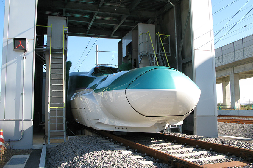
In 2022, for the first time, TSMC allowed a foreign company to take a stake in one of its foundries, in Kumamoto, having created a venture with Sony Semiconductor Solutions. Why do you think that Japan is such an interesting ecosystem for building a foundry?
For decades, Japan was a manufacturing powerhouse and the Japanese industry led the world in various applications, including consumer electronics and semiconductor products. This was achieved thanks to Japan’s strength in developing advanced technologies and high-quality products.
While the role of the Japanese semiconductor industry is no longer what it was, Japan still has many manufacturers with strong semiconductor-related technological capabilities. If you combine that with Japan’s well-developed supply chain and highly integrated industry, it is no surprise to see that it remains an attractive location for opening foundries.
Although the country currently faces certain issues relating to employment and labor shortages, we hope that new technological innovations that integrate flexibility and creativity will provide solutions to these problems.
Looking at the future, what do you think will be the new vectors of growth in the semiconductor industry? Where do you think demand will come from?
I am not certain if my answer to your question is the correct one, but our business climate suddenly changed over the past six months. The effects of the COVID-19 pandemic on the global supply-chain combined with Russia’s invasion of Ukraine have led to wide-spread shortages of components, semiconductors and so on.
As manufacturers ramped up production to address these shortages, sooner or later, we are bound to face semiconductor overproduction. As a matter of fact, certain large companies have already started cutting down production. They see some signs of an economic slowdown, particularly affecting personal computers, smart phones and some entertainment devices. These makers are not taking as many semiconductors as they used to, and we have to be prepared to face this big change. I hope we are not running into a situation where we will also be facing an overproduction of devices.
I am convinced that large companies are already carefully reviewing their programs. I suspect that some Japanese companies will be asking: “Can we keep up with this kind of expansion over time? Or should there be a certain limit at which we should cut back a little bit? and have we already reached that limit?” The industry has to take a look at the whole situation and slow down a little bit from now on.
In the short-term, I believe that a slowdown will be beneficial and expected. In the long-term however, it is clear that the demand for semiconductors will continue to increase, there is no doubt. It is just a matter of time.
On the backdrop of trade tensions between Washington and Beijing, China’s ambition is to develop its own semiconductor technologies in order to become less dependent on imported goods. Do you believe that China will be successful?
20 years ago, the Chinese electronics industry could be defined as primitive. Their technology was backwards and years behind that of other countries. Over the last 10 years however, they caught up at an impressive speed. In all honesty, China’s pace of development is scary. The Government enacted important policies to make themselves independent and less reliant on foreign countries.
China’s aim is to become self-sufficient in terms of food, energy and semiconductor supply, and it will happen! They have the technology, the brains and the money to achieve their goals.
Now that Japanese and American companies are also trying to enhance their own production capabilities, they will not be counting on Chinese suppliers as much as they used to. These economies are trying to become more independent by further relying on their own manufacturing capacity.
The same thing is true in Japan. Demand is currently very strong and many players have been investing in expanding their national production to fulfill the demand of Japan.
It is a rule of life that business never stays the same. There are always big changes, up and down all the time. Throughout my life, I have witnessed this reality on numerous occasions.
As foundry and chip production capacity increases around the world, concerns on the environmental burden of these foundries arise. A normal foundry consumes more than two million gallons of water per year. It also deals with very toxic chemicals during semiconductor production. As a manufacturer of micro-particle and electrostatic removing equipment, how do you see the relationship between semiconductor production and the environment?
The world of semiconductors will continue to develop in an increasingly dynamic manner. For Hugle, which has been focusing on developing eco-friendly and clean technologies since its foundation, the future is even more promising. We have always taken a genuine stance on the issue of environmental protection, especially since we are in a business that affects the production environment and, by extension, the global environment.
No single country, yet alone a single company, is capable of resolving environmental issues unilaterally and instantly. Environmental regulations are occurring around the world, including both drought and flooding, as well as repeated mountain fires.
Those kinds of abnormalities have been increasing at an unprecedented pace in recent years. In my opinion, I do not think that is directly connected to semiconductor production, but I think it is a byproduct of the way human beings have been living over the past 50 to 60 years.
How does your equipment help to increase efficiency and lower the environmental burden of semiconductor production?
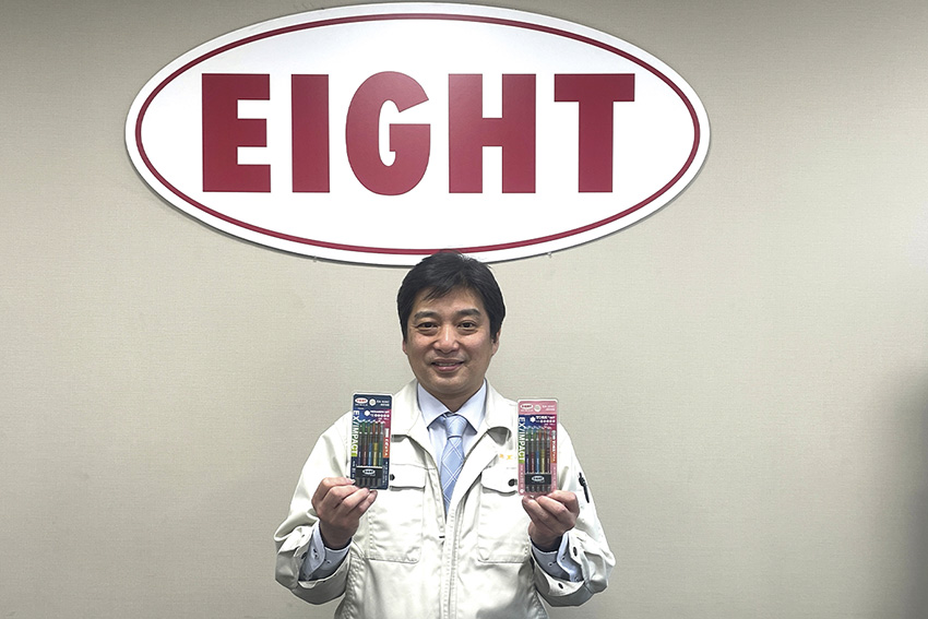
We are happy to announce our brand new cleaner, the SF-300. This new product is more compact than previous models but provides superior throughput. We have been able to almost double the productivity of the SF-300 compared to the old machines we have sold over the last 15 years.
In many cases, the time has come for our old machines to be replaced and I am sure the SF-300 will be well accepted because of its high productivity and the fact that it consumes less water, air and has a lower environmental footprint. By replacing old machines with the SF-300, our customers can double or even triple their production efficiency. This increase in performance will allow our clients to lower the environmental burden of their activities.
Furthermore, the product was developed based on the request of our Japanese customers. While foreign customers place greater importance on the price and specs of our machines, Japanese clients strongly consider the size and total dimension of the equipment. Japan has a limited landmass and therefore factory floors tend to be smaller than in other countries. Consequently, the new products that we release would be smaller in size to the previous models. If we do not achieve this compactness, our clients would have to redesign their clean room and factory floors.


When it comes to reducing the utilization of toxic chemicals, our products use as little organic solvents and neutral detergents as possible, and water and air are the main power sources. With the power of our proprietary technologies, we are determined to steadily pursue the path of becoming an "eco-friendly and environmentally friendly manufacturer."
What are some of the challenges that still remain in the field of micro-particle removal?
Naturally, the smaller the size of the semiconductor process, the greater the challenge. From a technical standpoint, we are still not satisfied with our technology and that is precisely why we are placing the core of our business on R&D. In February 2019, we opened a brand new R&D center to further bolster our development capabilities.
We are devoted to the constant improvement of our technologies and as such, we do not hesitate to invest our resources in R&D. Our employees are united by a common goal: creating something new. Improving our technology has always been our objective.
On top of removing dust and contaminants, our clients have recently been asking for technologies that will enable them to get rid of ammonia, hydrogen and other compounds. This process is focused on AMC removal and we have received various demands from the semiconductor industry.
While it depends on the nature of the device, there are other microscopic contaminants our clients want to get rid of. To address their demands at a molecular level, we are conducting a joint research project with a university in Kyushu. We are currently researching technologies for atmospheric airborne particle removal. These particles are so small that we must develop technologies at a molecular level… A challenging yet exciting project!
Customers have always asked us for our help to address their problems. For instance, the need to eliminate electrostatic discharges goes back to 30-40 years ago. Back then, electrostatic discharges represented tens of thousands of volts. We were successful in reducing the amount of discharges down to one or two volts, which is a tremendous achievement as far as I am concerned. Today, even greater control of electrostatic discharges is required by the industry.
What is the importance of creating joint research projects for your business? Are you looking for partners right now and if so, what type of partners are of interest?
We are always looking for new partners. For a small company like ours, there is always a limit to what we can do, so we have to rely on partners that have the technologies we require and the willingness to share it with us.
We are currently co-developing a new system with an American company. As we cannot make it by ourselves, we have been working with this new partner and sharing the development costs. Hopefully we will be able to introduce a new product to the market in the near future.
The buildup of static electricity in semiconductor manufacturing is unavoidable and is often a source of destruction for semiconductor devices. You offer a variety of ionizer products that can eliminate the buildup of static electricity. Could you explain to us how your ionizer products overcome this static electricity challenge?
To eliminate micro particles, we have to blow on the component and collect the micro dust from the surface of the wafer. Another potential danger is electrical discharge, which can instantly destroy circuitry.
Semiconductor manufacturers must maintain the level of ESD (electrostatic discharge) as low as possible. Today, this requirement is industry standard, but it was not as common back in the days. We were the first company to introduce ionizers that could lower electrostatic levels from 1-2kv to around 10v without contaminating the cleanroom environment.
When I started this business, customers often asked: “What are you going to do about static discharges?” I had a vision that dealing with electrostatic discharge would be required at some point in our business, and it did become a big deal later on so I am fortunate to have hung on to this business without giving up.
We raised the money, conducted experiments and talked to customers in order to get to where we are now. We are still working on a new product which will be introduced soon. We have high hopes for the future.
Can you tell us more about your R&D strategy? Are there any particular products that you are working on that you would like to share with our readers?
We do not see today as a time to simply increase equipment production capacity. Rather, we believe that today is a time of great opportunity. To further improve our quality of life, society requires us to develop new core technologies with a pioneering spirit. We must forget imitation and aim to develop next-generation technologies.
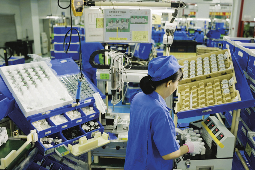
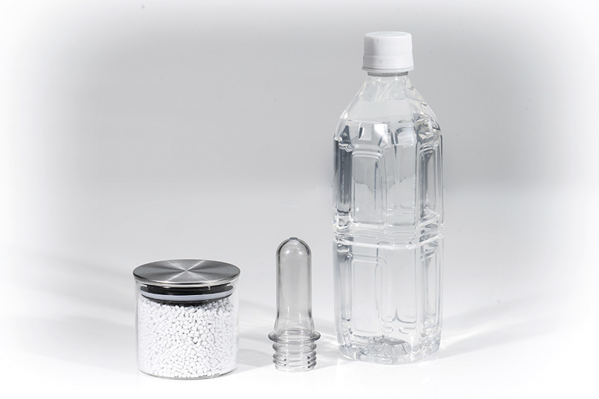
Hugle’s cleaning equipment is mainly utilized to clean the process inner containers (FOUP) used to store wafers in the 300mm semiconductor manufacturing process and to clean the shipping boxes (FOSB) used for transportation. In the manufacturing process of advanced semiconductor devices, extremely small amounts of contaminants can cause yield loss. As microfabrication technology advances, there have been increasing demands not only for removal of minute foreign matter inside containers, but also for removal of AMC and other contaminants that adhere to the inside of containers. To provide a solution to these issues, Hugle has established a proprietary degassing system and is also aiming to develop AMC removal equipment by applying its proprietary drying technology.
To achieve greater process control, there is a strong demand for control of contaminants not only on silicon wafers, but also on peripheral equipment. In response to this demand, we have been selling our own FOUP cleaning systems, UPC-12100/UPC-12500, throughout the world.
Another product is the Ultrasonic Dry Cleaner. This non-contact dry cleaner uses ultrasonic vibrating air to excite particles adhering to the surface of products before collecting them with a suction slit without scattering them. It also employs a circulating system that purifies the collected air and reuses it for discharge air. Since its launch in 1976, it has been used in production lines in a wide variety of industries, including the electronics industry, semiconductors, flat panel displays, printed circuit boards, and rechargeable batteries. For decades, we have worked strenuously to satisfy our customers' exacting demands in removing particles that are too small to see with the naked eye. As such, we routinely provide customized proposals for each problem and make improvements on our own products accordingly.
Recently, dust control in the rechargeable battery industry has become an urgent issue. Because the separators of high energy density batteries are becoming thinner, small particles on the electrode can penetrate through the separator and cause short circuits. As an answer, we developed a special cleaner which can remove particles on the electrode effectively.
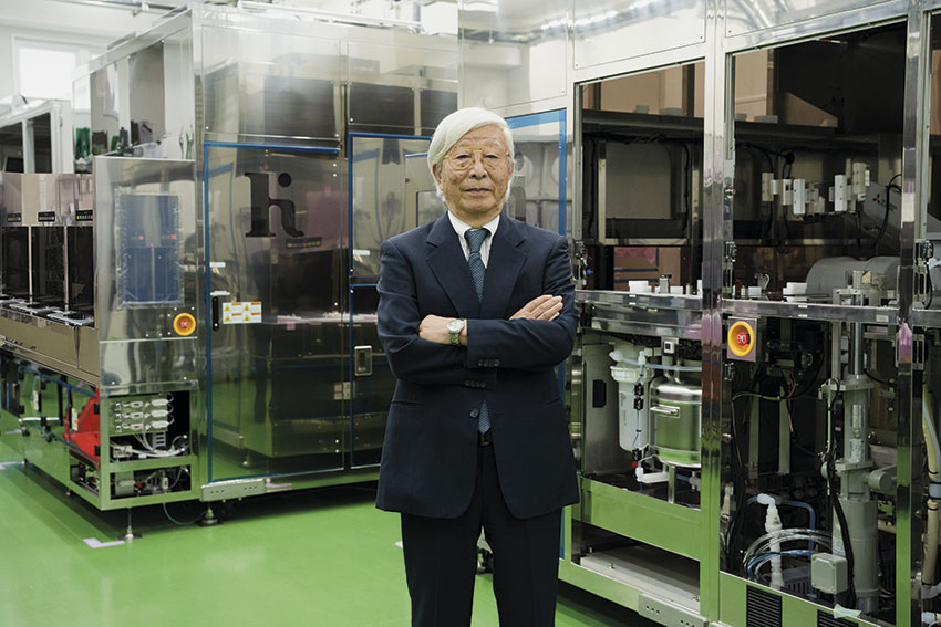
You mentioned that one of the big advantages of your company is the more than 50 years of experience and expertise that you have. What are some of the key milestones and important moments in the history of Hugle that you have lived through?
As I reflect upon my past, two moments happened to me that opened a window of opportunities. The first was when someone came up to me and told me about studying in the United States. Encountering new people and culture is an asset and a chance for all humans. The gentleman kept telling me to go to the United States, and I went. That was over 60 years ago and it changed my life, so to speak.
The second window was opened up by Doctor William B. Hugle who is the founder of SEMI and CEO of Hugle Industries. He asked me to work for his company as he was planning to open up an office in Japan to cover the East Asian area, including Taiwan and Korea.
Working at Hugle Industries was a big change of environment. Previously, I was just a big fish in a small pond but I was suddenly pulled out of the pond and thrown into a much bigger world. As much as it was a big challenge, it was one of the most important moments of my life. I managed to get through it and it brought me a great deal of experience, fortunately. Those were two unforgettable moments which led to new opportunities.
I often tell people, my own staff included, that if they do not like the company they are working at, they should go out and start their own. That is my philosophy. I always encourage people to go outside and to build their own future.
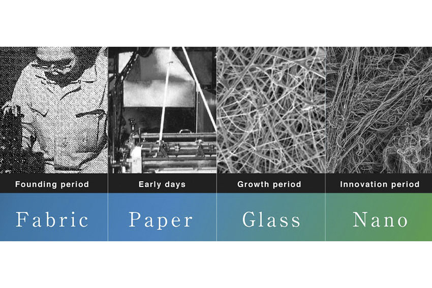
If we look at the company’s history: Hugle Electronics was founded in 1971 when The Far East office of Hugle Industries was reorganized as a Japanese corporation and began importing and selling Hugle Industries' products, as well as those of other semiconductor-related manufacturers.
At the time, Japanese manufacturers did not have IC processes or the know-how to use them, so they struggled to create mass production equipment. Subsequently, we developed our first in-house product, a wafer expander. By the late 1970s, domestic equipment makers had risen to prominence and it was no longer easy to sell imported products. In order to manage delivery schedules and to respond quickly to customer needs, the company transitioned into a manufacturer.
The "static electricity remover," "ultrasonic dry cleaner," and "carrier cleaning system" developed after that laid the foundation for today's products, contributing to the development of the semiconductor, FPD, and lithium-ion battery industries, and improving yields in cutting-edge microfabrication.
You mentioned at the start of the interview that Hugle’s success comes from its commitment to developing new products. From a management standpoint, how have you kept that culture of innovation alive?
I care for two things: customer happiness and employee happiness. I like to see customers with big smiles on their faces all the time. I always ask my people “Are the customers happy? As long as the customers are happy, you must be happy too! It is a combination of both of them. I tell them that if they take care of customers, the customers will take care of them.
What advice would you give to the next generation of Hugle executives or employees?
First, keep the customer happy as much as possible. Second, spend your life meeting a lot of people and experiencing various cultures. Take the time to explore new opportunities and things will develop from that point. I have seen many cases like this and I am sure the same thing will happen to my people too.


0 COMMENTS