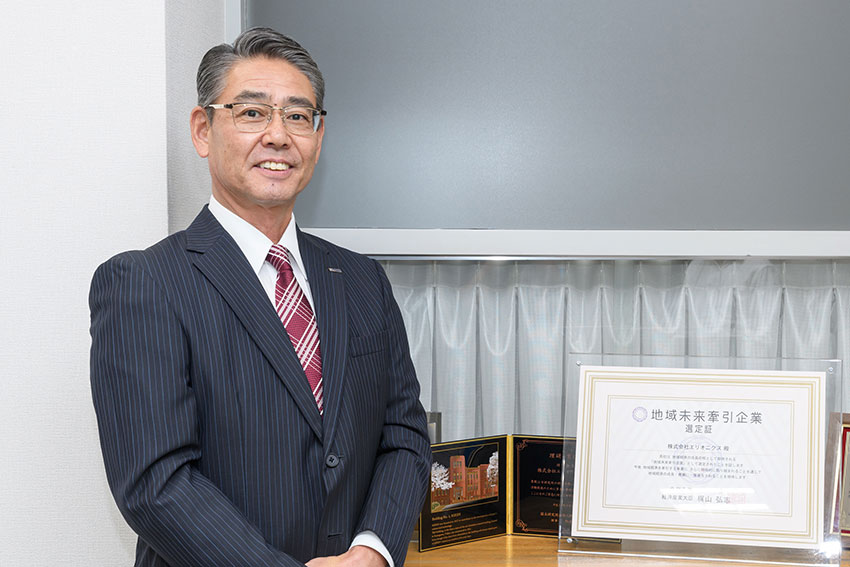
With expertise in nanotechnological devices, using electron beam lithography, Elionix is able to offer a variety of product line-ups to cater to its clients.
Since the end of WWII, Japan has had an excellent reputation for its attention to detail and the Kaizen philosophy of manufacturing has become famous worldwide. Nowadays firms are competing in a very competitive environment with Korean, Chinese, and Taiwanese manufacturers challenging Japanese companies. Yet, we still see Japanese firms retaining niche leadership in high-mix-low-volume sectors such as nanotechnology and electron beam lithography. Why are Japanese firms so successful when it comes to niche, high-mix-low-volume production?
I think a really good example that demonstrates this is in solar panels or LCDs. I do have to say that I think it is a mindset and a characteristic of the Japanese people that when we do something we go for a 100% yield rate. When we do that, the manufacturing costs go up, so it is not low. The mindset for monozukuri in Taiwan or China is different, where they will try to go for as low a cost as possible, and they don’t really care if the yield rate isn’t 100%. For them, the philosophy is to go as cheap as possible, and mass produce a lot of products. Once they reach the final inspection inevitably there will be defects and they will get rid of those.
I do agree that when you are aiming toward lowering the cost and going as cheap as possible, the Chinese philosophy is the best way to go. On the other hand, however, our mindset and characteristics aren’t really like that. The Japanese really go towards creating something that has a 100% yield rate from the start rather than cutting down during the final inspections.
Obviously, by doing this the manufacturing costs are higher, but we do still see a lot of users that are willing to take that price in exchange for much higher quality and products that are defect free. A really good example of that might be in the automotive industry, especially in the desert. You see that the Toyota Land Cruiser is really popular because they don’t break down, and I think that is why they have sold so many. I think the key and defining aspects of the Japanese brand is the high quality and the low to zero defects. This is probably why Japanese firms have been able to maintain their positions.
Back in the 1980s, companies such as Toshiba and Fujitsu held huge market shares in memory, especially in dynamic random-access memory (DRAM). In the late 1990s and early 2000s, they lost significant market share to pure-play semiconductor foundries such as TSMC. Yet still today we see that Japan is dominating when it comes to machinery for semiconductor production as well as chemicals. Why do you think Japan has been so successful when it comes to machinery and chemical-based production for semiconductors?
As you said, back in the 1980s Japan became number one in terms of market share, but then after those regional players came like Taiwan, and most recently South Korea and China. I have to be honest and say that the market share has shifted over to them now. Semiconductors are said to be the rice of the industry, so it is an unfortunate thing, but on the other hand, Japan is doing really well in creating manufacturing equipment for semiconductors. Electrical components is also another field that we are really good at, with companies such as TDK leading the way. While it is true that semiconductors themselves have shifted away, the support in production is coming from Japanese firms, so I can say that still in this field Japan holds a strong advantage.
As you alluded to, the chemicals companies too continue to hold strong and we are finding that even China, which is creating semiconductors, cannot stop their imports from these Japanese companies. This really illustrates how we are supporting manufacturing in the field.
Semiconductors is an industry that is widely known to continue to grow exponentially, however during the last 3 years due to COVID we have seen massive chip shortages. As a result, we’ve seen regional pushes to revitalize production in the US and Europe. As this regional revitalization push continues to ramp up production in the US and Europe, what opportunities is this presenting for a company like Elionix?
It is not only about Japan, but again we have come to know that the supply chain is extremely important. Right now, what is happening with our company is that we can’t get hold of the units necessary for the devices. This trend has continued, and it isn’t only about the units but also the connectors too. Those connectors are also experiencing shortages and it is difficult to get a hold of them. As a company and as a country we have come to really realize the importance of a stable supply chain, and we are trying to act towards that. The US has passed the CHIPS and Science act this year, where now the US government has a sizable budget allocated for the manufacture of semiconductors within their own country. Japan is going through the same thing, and TMSC is working with Sony Semiconductor on a joint venture to establish a fabrication plant in Kumamoto. Operations are expected to start there in 2024 and it has seen a massive investment of JPY 800 billion already.
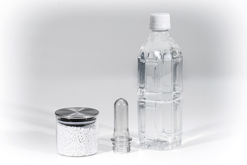
Your company Elionix has expertise in nanotechnological devices which use electron beam lithography. Most of your customers are in research and development areas, and you offer those customers a product lineup that includes such machines as your ELS-BODEN Series as well as the EIS Series of ion etching and deposition systems. Could you tell us a little bit about some of the unique features of these products and also some of the synergies you’ve been able to create for your clients by offering these different product lineups?
First of all, we have two divisions, firstly the measurement and analysis division, and then the nanofabrication division. The main system we provide would be in the nanofabrication division, and that would be our ELS series with the most recent unit being the ELS-BODEN Σ, which by the way accounts for around 60% of our total sales. It is our major product and is being used for various applications and is already utilized for cutting-edge research. We have received a lot of inquiries for the system to create quantum computing devices, so we see that field as having a lot of interest recently.
We also have the EIS series which is our ion-based system designed for etching and processing applications. By having the ELS and EIS series together we can utilize the ELS-BODEN for patterning and then after that, the customer can use the EIS for etching and grinding. Actually, we are the only company worldwide that has two of these types of equipment together. This is key to our strength, where we can provide the whole process, starting with patterning and going to etching as well. Another service we provide for our customers is a demonstration before purchase, which we see as a big plus in reassuring those customers.


Can you give us an insight into how you cater to those different mentalities in research and development when you compare a Japanese customer to an internationally prestigious customer like Harvard University, for example?
I think that ultimately they are the same, whether that is a professor coming from Japan, the US, Europe, or China. Without being able to produce results there really is no meaning. I agree with what you are alluding to, which is that the Japanese tend to be more process-centric. I personally believe that this is the reason why we tend to lag behind R&D when compared with other countries.
When we look at foreign countries, they really are results-centric and feel that those final results are the most important part of the process. For us to tackle this issue it is important to provide devices and systems that can produce results. We want users to feel joyful and happy because of our systems. I must stress that the devices and systems that we provide are not cheap, so with products that are not cheap we need to reassure those customers that we are giving them results, or else it doesn’t make sense for them to pay so much money. I personally really think that Japan should strive in this direction. I can say the same thing for the job itself here too. We are emphasizing the results side and I think this direction is the right one for Japan to take.
Can you tell us more about your latest developments when it comes to these industry demands for smaller and more miniaturized IC-based circuits?
That 2nm circuit revealed by IBM has yet to be put into practical use. TMSC right now is going through R&D and they want to make a product for 2nm by 2024. As for us, we have already been able to achieve 3nm, but we do believe there is a limit to how fine we can go. As a physical phenomenon, there is a certain limit, so now we must think about what added value we can provide to our devices. Our devices use one electron beam to do the patterning, and we think that the ultimate limit might be around 1.2nm High throughput is thought to be a value that we can add to our devices. This is all about being able to write faster and give high-performance positioning. We are shifting our R&D focus more towards this endeavor rather than continuing to go finer and finer.
New materials such as silicon carbide and gallium nitride are being developed as an alternative to silicon base material. When it comes to the handling of these wafers or chips, they are much more delicate than silicon-based ones as they are extremely thin. How have you adapted your devices to handle these new types of materials that are at the forefront of semiconductor production?
You just mentioned several types of material and yes you are right. The objective is a bit different for material, so I see that the things that can be done with silicon will be kept as silicon. In fact, that is what the customers want right now. Let's take for example gallium nitride, you will be able to create new equipment and devices that are unique and can only be made from this material. When we talk about fine patterning it doesn’t really matter which material we use, but I do want to talk about TMSC again because they are the most high-tech and most advanced company right now, and their direction is toward 2nm silicon. When you look at it, semiconductor processing from base material to ultra thin wafers has already reached the level of art because it really is that complex. Processing is being repeated thousands of times to do this 2nm process, and it feels like the absolute ultimate technology is being used. As you can imagine, what they are doing is very complex but what is being attempted feels like it is knocking on the door of the limit.
From your perspective with all of this development we have talked about, are you looking for any partnerships, either domestically or overseas?
Yes, we are. Basically, as I mentioned our products are for R&D equipment, so where we would deliver to would be the university professors and government research institutions, as well as corporate labs. Partnerships will result partially because we do have production equipment but this would also be to create communication devices for mobile phones. What is important for us is how we develop new systems or new devices and for that communication with end users is vital. Constant communication and exhibitions enables us to hear the opinions of not only end users but others that are in related fields. This is something we are always moving towards not only domestically but globally too.
One of the main fuels of the future is set to be hydrogen. The Japanese government has already said that 38% of energy must come from renewables by 2030. Japan already has the largest network of hydrogen fuel stations in the world, but there is a huge issue when it comes to hydrogen infrastructure called hydrogen embrittlement. We saw in our research that you provide a system called the Electron Beam Hydrogen Visualizer, and it is one of your newest products. Could you tell us a little bit more about this and how you’re helping to make infrastructure for hydrogen in the future?
Hydrogen is said to be one of the cleanest energy sources and what we want to achieve right now is the airlines, international ship routes, and city buses to transfer over to clean energy. This is where hydrogen embrittlement comes up, and we are currently working with the National Institute for Material Sciences (NIMS) in a joint research venture and we have actually already delivered one unit. This joint development is to visualize the mechanism of hydrogen impacting metal. Right now some of the professors have already started to analyze how the hydrogen is reacting, and it is vitally important as in the future metal is always going to be used in the storage of hydrogen. We want to contribute so that incidents don’t happen in the future and that is why we have decided to work with NIMS on this joint venture.
Are you looking to roll this machine out to international audiences or locations?
Honestly speaking we haven’t thought that far ahead just yet, but we have been thinking recently about ways to allow people to come in with their samples and use our equipment to provide visual data for them. This is because the equipment is quite expensive and we’re not sure how much researchers would be willing to spend in order to get that equipment for themselves. On the customer side, they are probably not sure how much efficiency is there right now. We have decided that the focus should be on providing this data based on the samples that come in. Of course, if such inquiries come in from foreign companies we will be more than willing to accept them and work with them.
In regard to your foreign operations, your company has a presence in the US and additionally partners in Korea, Taiwan, Singapore, and China. Moving forward, which countries or regions will you be focusing on in terms of growing your business internationally?
Actually, right now our production capability is pretty much full to the maximum already. We do understand however that if we’re able to expand and deploy our products overseas our sales would go up. One characteristic of what we provide is that we can’t just sell our equipment and that’s it. It just doesn’t work like that. We must secure maintenance towards the customer after dispatch, so this is one thing that is very important to keep our eye on. In order to do this, we need to secure service locations and this is the difficult part.
We have been receiving a lot of inquiries from India right now, so in the future, we want to be able to deploy to the Indian market as well. Unfortunately for China, there is some recent news from the Ministry of Economy (METI). Right now they are not granting us the permissions we need so we are not able to actively pursue sales activities there. We are already planning a new factory in Hashimoto and the idea is to make that factory double the size of our current plant. We want to make the size of the clean room double as well, and the reason we chose Hashimoto is that it is the location of the future linear rail. That linear rail will enable us to travel to Osaka in only one hour. We are looking at spring 2024 as the completion date for this new factory and we are excited about the increase in our production capabilities.
Imagine that we come back and interview you again on the very last day of your presidency. What would you like to say in that interview and what are your dreams for the future of Elionix?
First of all I’m not sure how many years I have left before I retire, but in March 2025 the company will celebrate its 50th anniversary, so 2025 will be a big year for us. Until then I want to keep on being the president of this great company and then after that who knows what will happen. For our 50th anniversary, my dream is to welcome that big year by opening our new offices and plant. My personal goals are related to growth, and helping the company to grow is extremely important to me. On the last day of my presidency, I hope to have achieved double sales and double the number of employees too. That would really contribute to the physical strength of the company. My mission is to be able to continuously provide equipment and devices that are really taken positively by all the academics in the world.


0 COMMENTS