For 70 years Advantest has been the most trusted and valued test solution company in the semiconductor value chain.
Since COVID-19, we have seen a huge disruption in supply chains for everything from cars to consumer electronics. This led governments and companies to become hyper-aware of the fragility of the supply chain. There was also a huge push to regionalize production. Between 2021 and 2023, 84 new foundries were constructed with an investment of 500 billion. If you talk about the US, the CHIPS and Science Act has seen 18 new foundries launched. With these vast developments in the last few years, what opportunities do regionalization and increased fabrication capacity present for companies like yours and Japan specifically?
I like to think of Advantest as already well-positioned. When we look at the footprint that we’ve established over many decades, and we map that to where some of the redistributions are happening, say it’s China for China or C+1 or T+1—those are common phrases now—usually, we look, and we see we are well positioned. For example, if there will be a new factory in Malaysia, we already have Penang and Kuala Lumpur offices. We are already established throughout Europe. We already have offices in Mexico. And so, although we’re not a huge company, our global footprint is pretty broad. I’ve had the good fortune since I took the CEO seat to travel around. I’ve seen, just in the last seven weeks, over 20 Advantest offices globally. We’re pretty broad, but we still have a small company feel, and the redistribution Advantest is already very well positioned. Part of the reason is that, unlike fab equipment, our customers are not only foundries and outsourced semiconductor assembly and test (OSAT) services but also design and system companies. So much of the movement and the supply chain redistributions are being driven not just by manufacturing but also by some of the upstream customers for a lot of reasons, so we’re fortunate to be already established with engineers, R&D resources, and field support staff around the design companies as they emerge in new regions or the well-established ones,
I would say that geopolitics and supply chain crunches have accelerated people to want to make sure they have a more resilient type of supply chain structure. I would also say that access to human capital, power, water, and natural resources are sometimes the driving forces behind some of the movements we’re seeing. There are certain places on the earth now that are constrained. There’s not going to be more power, and when big companies turn on, everyone goes dark except for that one company, so the customers in the supply chains are forced to look at moving elsewhere.
The last thing I might say is that what I see as a general trend is that design and software can go East-West quickly, but the supply chains, physically, have to be somewhat North-South, and they can be in smaller segments. For example, there’s a Korean supply chain, a robust Japanese supply chain, and, of course, Taiwan. Southeast Asia, Europe, and North America all have their own or are developing. It’s a very simple way to think about it, but the supply chains feel very much North-South, whereas innovation, R&D, and things like that can quickly move East-West.
In the 1980s and early 1990s, Japan held 50% of chip production capacity worldwide. That’s dropped severely, but Japan has shifted more into materials, equipment, and testing. With recent developments like Rapidus in Hokkaido and TSMC in Kyushu, Japan is pushing forward this idea of making it a regional hub for production. With the China and Taiwan dispute, many countries may see Japan as an alternative to Taiwan. Could you comment on that?
I think the manufacturing culture in Japan is almost second to none. You could argue for Taiwan, but the Japanese culture of manufacturing and execution is very high. What happened in the past with losing market share didn’t have to do with manufacturing quality. It had a lot more to do with the business model and some macroeconomic things that happened, and those things don’t exist anymore, so Japan is going through a renaissance now. As you pointed out, in the Kumamoto experience, the world watched as investment from government and industry went in together, and then eighteen months later, wafers were being produced. Hence, executing on a timeline is an advantage for Japan. And because that’s now understood, that goes into the formula for companies about where they want to expand and where the risk is, so the more Japan exhibits good execution, the more it will feed its growth and strength. And then you already mentioned access to best-in-class materials and equipment, and I think that will supercharge the manufacturing here.
I’d like to talk about semiconductors and, more specifically, the testing market. 2024 should be a year of rebound after a very difficult 18 to 24 months for the industry due to tightening monetary policy and a big increase in inventories, which saw the sector experience a plunge. However, if you take a macro look at it, between 2018 and 2023, the market for both memory and non-memory testers expanded on average by 30 to 35% every year. Advantest beat market expectations, hitting an expansion of around 60%. Last year hit the bottom in demand for testing equipment, and there is a lot of anticipation for when the rebound will happen, driven by new technologies such as GenAI and high-performance computing. How do you expect the markets to evolve in the short term and midterm?
Well, let’s first take a step back. When we look at things as a company, we look in three-year increments because we recognize that the industry is very cyclical, and it’s always been that way. There have been some vicious cycles, and this past cycle is not nearly as bad as we experienced. For example, the dot-com bust and the Lehman shock were vicious cycles. For us old guys in the industry, to have pretty good profit during this market bottom, we have a smile on our faces because of what we lived through in the past. That being said, 2024 looks to be flat or slightly higher than 2023 when we look at the overall market, and we disclosed that in our April disclosure. We see the system-on-a-chip (SoC) part of it being pretty flat. There are some bright signs right now, so we’ll see. As for memory, we see that as being higher because of the demand for the high-end DRAM memory needed for GPU and AI accelerators, so there’s a very high demand continuing in 2024. We have pretty good confidence that 2025 will be an up year as new capacity is coming online for wafer starts, and things like capacity in the back end should all drive growth in 2025.
One thing we always look at is the highest year of the previous three-year cycle, and our lowest year is higher than the highest of the previous three years, so you have this cyclical up and down. The trick for us is to invest through those lumps and not get overly excited when things go high or worry too much when things go low.
This year is starting to look better, and 2025 is looking better. However, we don’t have visibility into 20206 yet, so that’s kind of a short-term snapshot right now.
You mentioned that good signs are popping up for SoC and certain memory products. When you look at the revenue streams from the semiconductor industry, they were mainly legacy applications like automotive and consumer electronics. Nowadays, and NVIDIA is a great case in point, we’re seeing new technologies appear. In the next five to ten years, what will be the new applications or drivers of growth in the semiconductor field?
We usually see things play out in the cloud and in the data center, and that’s the case with companies like NVIDIA right now, so that’s going to continue. There are going to be new data center architectures, disaggregated, including architectures that leverage silicon photonics to do really interesting things in the data center space. But then I think what usually happens is that technology then moves into the edge environment, so when AI starts to be needed in edge environment use cases, that’s where the volumes go up. We love the data center business, and it’s very good for us, but mobility and consumer products drive equipment for the industry more than even high-performance computing. For example, notebooks, tablets, and phones that incorporate some AI will probably be a big thing. I don’t know if it’s beyond five years, but in the next 3 to 5 years, you’ll see a lot more of that, and that should drive a very good volume for the industry.
If we talk about the different parts of your business, your testers for SoC semiconductors are used to verify and ensure functionality, performance, and quality. This market is three times larger than the memory market. You’re catering to a variety of different players, from fabless manufacturers to OSATs to integrated device makers. Can you tell us how you’re able to cater to the different demands of those customers?
The company took a platform-centric approach where we built our test platforms so that the users, like the assembly and test guys, and foundries in some cases, can get a lot of reusability of the equipment by upgrading an instrument. For example, fabless Company A can use one configuration, and that tester could be reconfigured with some minor changes, while fabless Company B can use the same configuration. That approach started a couple of decades ago, and as that model proliferated into the space, even smaller fabless companies that weren’t even loading one tester could go out and find capacity in the OSAT space, and so it fed upon itself because, let’s say the company is taping out a new device and wants to find a tester that’s available for a couple of hours in the day. They would most likely use our V93000, which is our flagship SoC system. That model has just built upon itself.
Another key part for the SoC fabless companies wanting to scale is that we have test engineering partnerships. Right now, there are so many fabless companies emerging all over the place, and we have an ecosystem, so small companies can go to a company in our network and get access to engineers and testers to work on new products. So there’s kind of a ring around the Advantest inner ring that has test engineering and test development service providers who can cater to the smaller tier guys while we handle the larger, Tier 1 guys directly. That’s the SoC strategy that’s developed over time and works for us and it’s how we’re able to handle that kind of scale.
The memory segment is not that way yet. That’s dominated by the big names, and we’ve been doing business in both volatile and nonvolatile memory. We do volatile memory, which is DRAM, and nonvolatile, which is flash, and right now high-end DRAM is driving so much of the activity for us.
V93000 SoC system
Talking about high-end DRAM and high-end chips, when you look at testing within the semiconductor supply chain, there’s been a big evolution over the past 5 to 10 years. Before, testing mainly happened at two levels. You had testing in terms of design and evaluation, and then you had production testing, either wafer testing or end-of-line testing. Today, however, because of the complexity of these new chips, we see defects that occur after the chip is assembled or installed in the final product. As such, there’s an increased demand from manufacturers specifically for system-level testing or testing in an actual environment. How is Advantest reacting to this trend for new stages of testing, and how important is it in your future outlook to expand the semiconductor value chain in terms of different testing locations?
There are a couple of parts of the answer. One, for system-level testing, we made an acquisition in 2019 where we picked up assets from a company called Astronics for their system-level test business, so we’re now the biggest commercial system-level test player. And it’s interesting that now mobility devices, computing devices, automotive devices, and even memory devices are sometimes requiring this system-level test insertion for coverage. Sometimes, you need system-level tests because of the sheer number of transistors, so when they get to these advanced nodes, you can’t get to those using traditional scan vectors. You end up missing some small percentage of the transistors, which ends up being, in some cases, millions of transistors because a small percentage of billions is significant. You have to then run it through a mission mode or real native environment in order to exercise the device to get accurate quality.
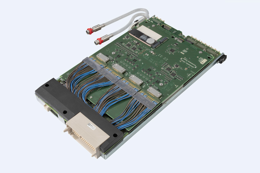
Link Scale instrument
The issue is that by the time you do that insertion, you’ve already invested in really advanced packaging, so everyone wants to move that system-level test further upstream, which we call moving left. There are a lot of efforts being made now to do things at the wafer or die level when you don’t always have the entire rest of the package together in order to run those system tests. We have worked together with our customers and partners to create solutions, and we have a new instrument that we call Link Scale, which is public, where we use peripheral component interconnect express (PCI-e) and USB ports to access and run some firmware types of tests in what would be like a native environment. There are also some other activities that we have in order to do those more functional tests further upstream.
A lot of it is working with the Electronic Design Automation (EDA) companies as well. It’s a huge challenge for the industry right now, particularly when the end devices now have average selling prices in the tens of thousands of dollars. It’s a challenge first to do that insertion to make sure they’re not shipping bad parts, but then to move that, and we’re fortunate that we have many different insertions. There are many wafer-level insertions, and now there are die-level insertions. There are burn-in insertions and final-test insertions. Then, there are system-level test insertions.
What we’ve done is to create an environment where we can do feedforward and feedback, and we have launched what we call Advantest Cloud Solutions. We have edge compute boxes and APIs and can give our customers connection points between the different test insertion points so that they can adjust where they want to place their tests. They can learn from failed devices and move those tests, sometimes even adaptively, where real-time data infrastructure with millisecond-level latency is used to change the test model while they’re testing. It’s very advanced.
I’d like to delve a little deeper into some of the technical issues that you’re helping clients overcome. If we talk about something like high-performance computing (HPC) and GPUs, an obvious issue is overheating because of the high power consumption. If we talk about signal integrity, we see voltage drops or electromagnetic interference (EMI) as other technical challenges. Then, of course, you need to test these in real-world environments, like extreme low and high temperatures. How are you able to replicate such real-world environments in your testing, and what are the most pressing technical issues that you’re helping your customers overcome?
We don’t just have to replicate what the device is going to see. We have to go beyond that. For example, for something that may see one kilowatt in a data center, we have to test for higher because there are all kinds of spikes that it’s going to see, and we have to test that. It’s a lot of technology development, and we don’t always have it, so we partner in some cases, but you hit most of the key ones. I would say thermal and power are really at the top of the list right now, and the ability to actively control the device under test while going through these really vicious power cycles is a real technical challenge. You’re seeing all kinds of techniques that involve our entire portfolio and really take us to more of a test solution, which is where we’re heading as a company.
A big theme for our company, and maybe this is a bit of a tangent, is that the complexities of the devices now require us not to think about just a box or a piece. Now we have to think about it holistically, so you have to be thinking about the power supplies and things like pre-triggering temperature control. Then, you have to have the most advanced thermal interface materials. You have to tackle it on the top and the bottom of the device. You have to use analytics to make sure that you’re not going to get burns, or if you are, you have to pick that up and do preventive kinds of things because this is very high stakes, and all the pieces are very expensive in this. The biggest challenge for the industry right now is handling these HPC devices that are super high power.
You mentioned taking this holistic approach. One of the big focuses that you’ve had over the past years was to enhance your engineering capabilities, not just in terms of maintenance but also in helping your customers increase yield, set the machine within the fab, etc. How do you to move forward and evolve, not just as an equipment maker but also as a service provider to your clients? How important will that be in the achievements of your vision?
Regarding the part of the services, I don’t think any semiconductor capital equipment company does a good enough job of actually getting the value back on the service side. It kind of gets lumped into what we provide as the hardware capital equipment, but we are seeing more opportunities to do things like preventative maintenance and health checks, as well as work with our partners to develop some software solutions. We are selling subscriptions now for things like data infrastructure and machine learning operations (MLOps). These are not our traditional services, which are more like maintenance, replacing instrument cards, and uptime. But there’s another level of service now where you can add true value, and the customers are willing to pay for that value because it either helps them in their time to yield or their time to market or just some economic savings so that they are willing to now look at things differently.
We’re not anywhere close to where we want to be, but I think we’re starting to see the industry put more value on the services piece, back to the equipment guys. It is not just us but all the front-end and back-end assembly people and the data that you can get from each of these insertions is really rich. There’s the device data that our customers own, but there’s a bunch of equipment data that comes from the entire test cell. When you marry the equipment data with the device data, you get a lot of value and can solve a lot of problems. In some cases, cooperating on data and data rights becomes more complicated than using actual technology. The legal folks worry about who owns what and whose IP is whose, but we’re getting there, and we’re starting to do projects to work with customers and suppliers.
I’d like to talk more about the company's plans. We mentioned expanding the value chain of testing and engineering capabilities. A third option we’ve seen over the years is to expand into other related fields. I think the best example of that has been your foray into what you call nanotechnology, which is really your scanning electron microscope with your proprietary beaming technology. If you look at this piece of equipment, the main use case should be for extreme ultraviolet (EUV) lithography, specifically at the mask level. Aside from TSMC and, more recently, Intel, nobody is really using EUV yet. The costs are very prohibitive and the productivity and the technology don’t allow it to beat the traditional UV lithography, which is still increasing year after year. Regarding these new investments, specifically nanotechnology, when do you expect this to pay dividends, and how do you think EUV might transform or impact the Advantest business?
Our nanotech group is actually a pretty mature group. It’s not a new investment. We’ve had it for quite some time now. The nature of the mask house is that the markets for Critical Dimension Scanning Electron Microscope (CD-SEM) and defect review SEM are not going to explode suddenly. It’s a very steady level of business, and for us, it’s a very healthy business, albeit not anywhere close to the core products on our tester side. But we service legacy nodes, through the 193i lithography technologies, so we measure lots of masks, and we are always being challenged to do it faster because there are just more and more masks in the world.
As far as EUV, we already have EUV CD-SEM and DR-SEM machines, and right now, we are qualified for the High NA EUV, which is just one guy installing it. That’s very important, I think, for the future, and the technology used to accurately measure the CDs on the High NA EUV mask is something important. This for us is still metrology, so it fits into our test and measurement, and I believe someday people will look at the imaging on the mask measurement and be able to connect it to the electrical test. The very first part of the semiconductor happens at the mask, and then we have all the way to the system-level test, and there is a relationship, for sure, about how you print these masks and the features on a mask because they end up somehow affecting the electrical quality. So I’m never going to lose the dream, and it’s maybe the Holy Grail for the company, to somehow connect the very beginning to the very end. I love the technology, and it’s really important for us to continue to invest and see what’s happening on the front end, what technologies are coming, who’s going to go first on this or that node, and we use that to help inform us about where we want to put our investment on the back-end side. It’s not going to be huge for us, but it’s a jewel in the company.
I want to ask you about human resources, which is a big part of your business. As a Japanese company, you have to deal with a declining and aging population locally, and there’s huge competition for graduates and for securing human resources for the future. How do you cope with that?
Depopulation is affecting developed countries all over the world, be it Korea, Japan, Taiwan, or Germany, it’s a global issue. I think that’s why there’s going to be more emphasis on AI: productivity needs to improve with this declining population. That’s also why you’re seeing this redistribution of supply chains to go where there are more people for the fabrication of things, so it’s a challenge that we recognize. It used to be more challenging for us to hire people because we were competing as a smaller company with big-name companies. Now that we’re bigger and we have some of the most valuable companies in the world as customers, it has become a little easier for us to attract young talent, and we make sure we market ourselves that way for sure.
We’re also making an effort to get into universities around the world. We’re developing and have developed a curriculum for universities where we run test engineering. We work with the deans in schools, and we develop curriculums. In that way, we develop young university students; they come in and work as interns, go back and finish their degrees, and then we hire them. It’s a nice process where you’re guaranteed to have quality engineers, but I also think it’s going to be a big challenge, and we’re going to have to adopt more efficient practices to get more out of our talent. We can’t just approach it with a mass workforce.
Does that encompass cloud services, like doing things more remotely for your business model?
There’s going to be more cross-world collaboration for sure, but we have a lot of projects where we’re using the basic things like Copilot, and we’re also doing code generation and using AI to design our own application-specific integrated circuits (ASICs) that go into our own test instruments. We are also applying AI to manufacturing and yield learning and for our administrative functions, like moving from quote to cash processes. We’re using a lot of digital transformation methods to generate more efficiencies. It will be a combination of continuing to attract the best talent, working across the world in a globally distributed nature, and getting better efficiencies by using digital tools.
You have announced the Third Mid-term Management Plan in June. Could you tell us what the key theme of the plan is?
The key theme is 'complexity.' There are two aspects. One is technological complexity, such as gate all-around (GAA). The other is geopolitical complexity. Rising geopolitical risks have led to increased semiconductor production capacity and geographical re-distribution.
The growing demand for high-performance semiconductors, which require high technology for manufacturing, and the diversification of value chains are bringing this “Era of Complexity” to the semiconductor industry.
I see this as an opportunity for our company to grow further and Advantest’s role is becoming increasingly important in this new global business environment.
We believe that efficiency is the key for addressing it. To realize the significance of efficiencies, we will pursue the next layer of automated testing to help our customers release their products into the market in the most efficient manner possible.
You have done some big M&A deals. Essai was a very important one, and last year, there was the Taiwanese company Shin Puu. You also invested in a power semiconductor firm in Italy. You mentioned that the focus is now on stitching, but do you have any plans to continue M&A in the upcoming years? Is there perhaps a particular sector that you’re targeting to help the stitching happen?
I’ll just say that where we have any gaps in technology or supply chain, we will be aggressive through either investing or partnering. I really can’t say more than that. We feel they’ve done a pretty good job, but there are more things that will show up as gaps, and I think there will be a lot of partnerships because we’re starting to bump up against adjacencies that are large. You know, we’re not going to get into the EDA space, for example, so we have to collaborate with those companies. We’ll pick up what we need and collaborate where we need to as well.
You explained the very strong international network that Advantest has been able to build. You have a big focus, in terms of revenue, on the Asian region, which has a strong presence in the big fab countries like Taiwan and South Korea. If we consider all the changes that are happening in the world and the expected increase in production in the US and Europe, how do you foresee your international expansion moving forward, and what markets do you think will be crucial for growth?
I don’t know, but I think it’s going to be everywhere. There are things coming up right now in North Africa and Australia. India is an emerging area as well. I don’t know that there’s going to be one area, but what I can see is that there are regions that have certain domain competencies, so if there’s a region that does very well for automotive, then you’re going to see the supply chain focus on that area. Europe is a great example. So you’re going to see a lot of these domain-expert end markets, and you’re going to see the semiconductor people start to move around those markets. Then it’s a cascade, and then all the rest of us start to follow. That’s how I envision things. The world is going to have areas of expertise or centers of excellence for end markets, and you’ll see people set up around that.
I have one last personal question. You were recently named CEO. Now that you’re at the beginning of this journey, is there a goal or an ambition that you want to achieve during your tenure?
I’m an engineer, so when I talk about us laying the groundwork for solving big industry problems, as an engineer, it’s only satisfying when you put it all together. It’s not satisfying for me yet. So, at a high level, the engineer in me wants to see these cross-functional pieces start to work together. That’s more on the technical side. On the broader culture side of the company, we are a seventy-year-old company that was born in Japan, but more than half of our employees are outside of Japan, and 96% of our sales are outside Japan. The only place we speak Japanese, which I can’t speak, is in Japan. But our roots are in Japan, and I have a commitment to never let the company get separated from its original Japanese roots because I feel in my heart that the culture of Japan is second to none in the world. As a CEO, I need to make sure that I remember where we came from.
I have been in the company for almost 26 years now. From the outside, it seemed like it was a really bold move to appoint me CEO, but from the inside, I’m just an Advantest guy. And we have made bigger, bolder moves in the history of the company, much bigger than appointing a person who spent his whole adult life in the company as a CEO. To us, it’s not a big deal.
For more information, visit their website at: https://www.advantest.com/en/


0 COMMENTS