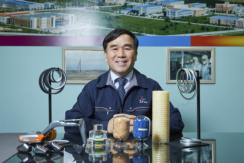
Hanamicron, Korea’s leading OSAT, is utilizing its partnership with Samsung and its expertise in ultra-thin wafer technology and particle dynamics management to drive global expansion.
Through the success story of Korean MNCs who have dominated both consumer markets and high-tech industries, Korea saw the emergence of domestic suppliers. As the Korean industry continues to grow into a key global player, critics claim that the SME sector might find itself ‘sandwiched’ between new and established manufacturing powers that will limit their international expansion. To what extend do you agree with this argument? How can SMEs better diversify their client base and reduce their dependence on Korean MNCs?
Recently, there has been considerable discussion regarding the semiconductor ecosystem in Korea. The root cause lies in the fact that despite significant advancements in the Korean semiconductor industry, its ecosystem hasn't achieved robustness. I fully align with the argument that Korean MNCs are caught between established economies like Japan or the U.S. and emerging ones like China. This situation arises from the distinct trajectory Korean semiconductor companies have pursued, differing from counterparts in Taiwan or the U.S. Notably, memory semiconductors have spearheaded Korea's semiconductor ecosystem, largely due to the unique features of IDM, which offers a comprehensive solution from design to production, proving highly efficient for Korean customers. Consequently, significant capital investments from conglomerates have flowed into memory semiconductors.
Expanding upon IDM's unique features, I perceive this as the primary determinant. However, major companies like Intel and TSMC operate differently. Despite their semiconductor industry dominance, they also prioritize nurturing the broader semiconductor ecosystem. For instance, Intel's growth, primarily driven by CPUs, extends beyond its role as a major IDM player to actively fostering equipment, materials, and the overall semiconductor ecosystem. Similarly, TSMC, a key player in semiconductor manufacturing, focuses on the front-end process or fab, thereby enhancing professionalism within their ecosystem while supporting the semiconductor industry at large.
Conversely, Samsung and SK Hynix have emphasized IDM as the optimal approach, diverging from the broader ecosystem cultivation seen in Intel or TSMC. This resulted in a relatively underdeveloped semiconductor ecosystem in Korea, heavily reliant on established players like Intel. Moreover, limited international cooperation further hindered progress. Another significant challenge arises from intense competition between these conglomerates, forcing companies to align with one ecosystem, constraining SME growth.
I firmly believe that for an ecosystem to flourish, it must adopt an open-source approach, fostering overall growth. However, the hierarchical nature of Korea's ecosystem presents a formidable obstacle, challenging to overcome. I tread cautiously, recognizing the potential sensitivity surrounding criticisms of conglomerates.
In 2022, during a period of chip oversupply and reduced production, SK and Samsung scaled back orders in Korea, leading OSATs to operate at only 50% capacity. Concurrently, SK entered into a partnership with TSMC for AI chip production, with TSMC handling backend processes. How crucial is it for companies like yours to diversify beyond servicing only Samsung or SK, and instead cater to international IDMs to mitigate cyclical risks?
I believe there has been a notable shift within the Korean ecosystem towards embracing open-source principles, reflecting the prevailing trend in our development approach. Encouragingly, Samsung and SK Hynix are also transitioning towards an open-source ecosystem. This transformation stems from significant challenges faced in 2019, including Japan's unilateral export restrictions, prompting Korean companies to adopt a more competitive and collaborative stance. Historically, domestic memory OSAT companies primarily served SK Hynix and Samsung, often facing a binary choice between the two. However, Hanamicron, like others, is now navigating a landscape of collaboration with both SK Hynix and Samsung, demonstrating a more diversified approach.
Yet, in the context of global counterparts, Korean companies still contend with perceptions of hierarchical and vertical structures. Overcoming these stereotypes presents a primary challenge. Once we transcend these constraints, we can genuinely compete in international markets. Despite operating on a smaller scale compared to SK Hynix or Samsung, Hanamicron is expanding our portfolio by engaging with U.S.-based fabless companies such as NXP or Microchip Technology. This diversification strategy underscores our path to expanding our business footprint.
In recent months, international governments have rolled out trade policies aimed at promoting supply-chain realignments. The best examples have been the Biden Administration’s Inflation Reduction Act and the Chips Act, which are offering billions of dollars in subsidies to American companies and trade partners for the development of technologies key to innovative applications, such as clean energy, battery and semiconductors. These policies are creating opportunities for Korean enterprises, as it positions them as an attractive option for the creation of compliant supply-chains. What opportunities does this global realignment create for Korean companies?
I believe the IRA and the Chips Act in the U.S. offer significant opportunities for Korean companies. Firstly, as Samsung and SK Hynix expand into the U.S. and Western markets, they seek to bring their OSAT partners along. While direct discussions regarding our expansion into these markets may not immediately impact us, there are potential indirect benefits, such as utilizing sites in locations like Vietnam.
The focus of the IRA and the Chips Act primarily revolves around foundries, necessitating new forms of collaboration within a fresh ecosystem. I anticipate that the role of Korean SMEs will become increasingly vital in this context, prompting Korean companies to invest considerable effort in this direction.
Over the last decade, demand growth in the electronics and semiconductor industry was mainly driven by applications such as smartphones, consumer electronics and automotives. As new technologies, including AI, 5G and the Metaverse become mainstream, observers expect major changes in revenue streams. For example, NVIDIA Corporation, which has grown into a global leader in the production of AI microchips, saw revenue increase of 50% from the previous quarter. Looking at the next 3 to 5 years, what main technologies will be the new vectors for growth?
From my perspective, the primary growth drivers for the semiconductor industry will be AI, mobility solutions, including advancements in vehicle technology, and telecommunications. The increasing complexity, data load, and demand for miniaturization will play pivotal roles, all of which are closely linked to packaging technology. Historically, we addressed complexity issues through System-on-Chip (SoC) designs, attempting to integrate all components into a single semiconductor. However, the challenges in investments and yields have constrained the further expansion of this approach. Consequently, we are transitioning towards System-in-Package (SiP) systems, with 2.5D technology emerging as a fundamental component. Within the realm of 2.5D technology, segments such as interposer and substrate technologies will hold significant importance.
In addressing the surge in data loads, high-bandwidth technologies like High Bandwidth Memory (HBM), rapid testing techniques for HBM, and Automated Optical Inspection (AOI) measurements will be crucial. Furthermore, for miniaturization, key technologies such as multi-stack ability, or what I would term as 3D, and ultra-thin wafer technology will be essential. Notably, recent achievements in reducing wafer thickness from 300 to 30 microns highlight significant progress in this area. To excel in these processing technologies, particular attention must be given to particles and alignment.
Given these technological imperatives, I believe that over the next three to five years, advancements in packaging technologies will be of paramount importance, shaping the focus of our research and development endeavors.
When we trace the evolution of packaging technology, it's evident that it has undergone numerous phases. For instance, flip chip technology, initially introduced by IBM, fell out of favor before experiencing a resurgence, catalyzing growth. ASE's success story, fueled by wafer-level advancements, further exemplifies this trend. As we enter the era of 2.5D and 3D architectures, how is your company strategically positioning itself to leverage this moment and propel the next phase of growth? Additionally, how do you assess your competitiveness in developing this technology compared to other OSATs?
Reflecting on the trajectory of technology, IBM's contributions, which date back four to five decades, are currently experiencing a resurgence. Our company has been harnessing 3D stacking technology for nearly a decade now, particularly evident in our success with Multi-Chip Package (MCP) stacking of up to 16 layers. Thus, we possess substantial expertise in 3D technology. However, the primary challenge lies in aligning the right technology with specific applications.
In the dynamic landscape of the memory semiconductor industry, the focus has shifted towards application-specific needs and the interplay between CPU and memory. The market demands solutions capable of handling increasing complexity and high-bandwidth data processing. Identifying the most suitable technologies for specific applications is paramount.
We stand competitively equipped in the market, leveraging our advanced technologies. Yet, it's worth noting that while we excel in 2.5D applications, we lack experience in large body or high-bandwidth production. Despite this, we are actively working towards mass-producing CPUs and application processors (APs) integrated with memory in the realm of 2.5D. Our competitors, such as Nvidia, SK Hynix, and TSMC, have successfully ventured into 2.5D production, with TSMC introducing its proprietary CoWoS technology. This technology is also in our pipeline, and we anticipate being able to mass-produce it in the near future.
Your industry is known for its high-pressure environment, constantly demanding more data from smaller and cheaper chips—a trend that has persisted for the past three to four decades since Fairfax initiated packaging. You mentioned AI as a significant topic of discussion. How do you foresee AI impacting your future, particularly concerning SiP and related technologies?
Recently, AI's integration with semiconductors has been a prominent subject of conversation. While AI chip applications, particularly those embedded in mobile phones or vehicles, are gaining traction, widespread adoption may take time. However, what's crucial is the growing recognition among the general populace regarding the importance of AI technology. This recognition is especially pronounced in fields such as translation, interpretation, autonomous vehicles, and robotics, which are poised for significant advancements.
Traditionally, semiconductor growth has been driven by PCs, mobile devices, and vehicles. However, the emergence of AI chips and device memory, while not directly tied to these sectors, will inevitably intersect with them. Even if not AI per se, functionalities like signal processing integral to AI will influence applications in PCs, mobile devices, and vehicles. Furthermore, the future of services is anticipated to rely heavily on server connectivity, necessitating smoother interactions between CPUs and servers for consumers.
The demand for AI chips in mobile devices, vehicles, and IoT-related sectors is expected to surge. Currently, meeting these demands primarily focuses on servers. However, as applications diversify, there will be an increased need for AI-driven solutions. Our outlook for the future includes collaborating with Samsung on packaging tests, particularly in light of their recent release of the Galaxy 24, marketed as an AI phone. As functionalities of application processors (APs) and mobile devices expand, we anticipate a corresponding rise in demand.
Hanamicron is composed of several subsidiaries. Notably, Hana WLS, the wafer level specialized division, spun off in 2021 by dividing the bump and wafer test business division. Additionally, HanaMaterials is specialized in silicon wafer manufacturing and silicon parts. What synergy do you create between Hanamicron and the subsidiaries to promote innovative technologies?
Let me first address the relationship between HanaMaterials and Hanamicron from the perspective of our founder. HanaMaterials was initially established as a new venture in the front-end process. However, given the intense competition in silicon wafer manufacturing, particularly dominated by U.S. and Japanese peers, it was challenging for us to establish a foothold. Consequently, we shifted our focus towards materials used in plasma etching, specifically silicone ring materials. Notably, HanaMaterials boasts the production of the world's largest silicone ingot, measuring 600 milliliters. This distinction underscores our position as a leading global manufacturer in this domain.
Now, allow me to elaborate on the synergy between Hana WLS and Hanamicron. When I joined the company in early 2019, I observed that our portfolio was excessively reliant on memory semiconductors, leaving us vulnerable to market volatility. Recognizing this vulnerability, especially during a semiconductor industry recession, I pivoted our trajectory towards microelectronics. To achieve this, I believed it was imperative to establish a testing and bump business. Moreover, amidst discussions of Samsung launching its own foundry business, I foresaw an increased reliance on the external ecosystem, presenting significant opportunities for us. Hence, I initiated the launch of the bump and testing division to capitalize on these prospects.
To meet the growing packaging demand, in 2020 and 2021, Hanamicron invested more than USD 140 million with the goal of positioning itself as a major system OSAT provider. Today, Hanamicron offers large packaging technologies such as flip-chip, wafer level, and SiP, operating in-house bumping and cutting processes, as well as an optimal testing platform that handles the testing program, probe design, and the test itself. With this turnkey solution, how does this position you as a major OSAT in the international markets?
Over the past three years, our steadfast pursuit of this goal has begun yielding tangible results, particularly evident in our burgeoning partnership with Samsung, which is reflected in our financial performance. While our collaboration with Samsung has been fruitful, establishing partnerships with major fabless companies like Qualcomm or NXP, primarily based in the U.S., presents ongoing challenges. However, if our endeavors with these key players in Western markets gain traction and reach full fruition, it will serve as a catalyst for our global expansion, albeit this may take time.
Indeed, recent visits from major fabless companies in the Western market have shed light on two primary concerns. Firstly, there's the perceived risk associated with operations in China. Secondly, our partnership with Samsung Foundry raises questions about our independence and potential conflicts of interest. Historically, global fabless companies leveraged Samsung Foundry's internal infrastructure. However, as Samsung Foundry pivots towards focusing on FAB front-end processes and outsourcing assembly and testing lines, we see significant opportunities emerging to secure orders from these global fabless giants.
In discussions surrounding 3D architecture, a pivotal aspect is the ability to interconnect different dies through a silicon interposer. Is HanaMaterials also making strides in supporting our efforts towards 3D architectures and SIC?
HanaMaterials primarily focuses on manufacturing silicone rings and wafers for plasma etching. These silicone rings serve to safeguard the gas and electrodes of the wafer during the etching process. However, when it comes to interposers, a different type of wafer or substrate material is required. The properties of HanaMaterials' wafers differ from those of standard wafers. While typical wafers boast a purity level of ten-nine, HanaMaterials' wafers exhibit a higher purity level of seven-nine. Consequently, they may not be suitable for use in conventional chips.
Your company has experienced remarkable growth over the past five years, with the first three quarters of 2023 surpassing expectations, despite a slight downturn in the fourth quarter. Reflecting on this success, what do you attribute to your company's accomplishments? Looking ahead to the next five years, what key aspect of your business do you anticipate will be the primary driver for growth?
The cornerstone of our success lies in the strategic diversification of our product offerings and business portfolio. Initially, we transitioned from the memory semiconductor sector to system semiconductor, thereby expanding our testing business. While unforeseen challenges like the China risk emerged, I deliberated on enhancing our company's competitiveness. This led to initiatives such as acquiring global insights and expanding our presence with a branch office in Vietnam.
Over the next five years, our foremost objective is to bolster our competitiveness as a global OSAT company. This entails ensuring that our technological capabilities, workforce, and turnkey solutions are aligned with international standards, exemplified by industry leaders like the U.S.-based Amkor. While strides have been made in growing our employee base and operational capacity to global standards, the challenge lies in enhancing our technological prowess.
Historically, our expertise has been concentrated in the memory semiconductor realm. The key technologies underpinning microelectronics and memory semiconductors largely overlap. Our company excels in manufacturing ultra-thin wafers and managing particle dynamics, areas where our capacity shines. Yet, our primary focus now is on bridging the gap between major fabless companies worldwide and our technological capabilities, while strengthening the synergy between their applications and our technology.
In the past, such opportunities were scarce. However, with Korean companies fortifying our foundry ecosystem, we anticipate more avenues for collaboration between U.S. companies and Korean counterparts. I firmly believe that this vision will materialize within the next one to two years.
You recently closed a billion-dollar investment in Vietnam, and you also have a presence in Brazil with factories and sales operations in the U.S. Over the next five years, how do you envision the evolution of your geographical footprint, both in terms of production capabilities, currently centered in Vietnam and Brazil, and in sales, particularly with major U.S. fabless companies?
We currently operate two factories in Vietnam, one in Bac Ninh, established a decade ago, and the newly invested $1 billion facility in Bac Giang. Additionally, we established a factory in Brazil a decade ago. However, focusing on domestic geography, I envision developing our company into a hub for comprehensive turnkey solutions.
Given our proximity to Samsung and SK Hynix plants here in Korea, we will continue to mass-produce high-end products and maintain the current status quo. However, at our Bac Giang plant in Vietnam, which is dedicated to SK Hynix, our partnership will persist for the next seven to ten years. Currently, production stands at 50 million units per month, expected to grow to 200 million.
Meanwhile, our Bac Ninh facility in Vietnam is geared towards microelectronics. We plan to expand this business, particularly focusing on System in Package (SiP) solutions. Projects from foreign fabless companies will continue to operate within our Vietnam-based plants.
The business model in Brazil differs significantly from that of Korea and Vietnam. Dubbed the "wafer business model," our Brazilian operations involve purchasing wafers, packaging them, and marketing them as local or indigenous brands, benefiting from tax incentives. We aim to further expand our wafer business model in Brazil. Should the foundry business expand, we will leverage our expertise and experience in Brazil to strengthen partnerships and consider direct investments in the U.S. We remain flexible to adapt these business plans based on evolving market dynamics.


0 COMMENTS