ULVAC-PHI, born from a strategic collaboration between Physical Electronics and ULVAC, leverages market-driven innovation and cutting-edge surface analysis technology to expand its global footprint and achieve unparalleled success in diverse industries.
Right now is a pivotal time for Japanese makers. Policies like the US Inflation Reduction Act are forcing corporations to diversify their supply chains for reliability and to reduce country risks, with nations like Japan known for their reliability, advanced technology, and a weak JPY. Consequently, Japan has never been a more cost-effective option. This means that Japanese firms have an opportunity to expand their existing global market shares. Do you agree with this sentiment, and in your opinion, what do you believe to be the advantages of Japanese companies in this current macroeconomic environment?
I think it would be good to premise this initially as how we’ve developed as a company. ULVAC-PHI is actually a company that was based on a US company called Physical Electronics. From that perspective, our major business was dealing with the United States, and from that core, we are now steadily starting to expand to other countries.
When it comes to procurement and our supply chain, the majority of that has been based in the US with our subsidiary Physical Electronics USA. At the same time, we are slowly expanding and diversifying our own supply chain when it comes to the procurement of materials, starting with Japan, of course, and then beyond the US to other countries like China. Right now, we have a special initiative underway within the company to seek good materials in a speedy and affordable manner. In a sense, we function as a part of the ULVAC Group, but our role goes beyond merely supporting the ULVAC Group. We actively utilize the ULVAC Group's supply network. This strategic approach aims to have a significant impact on the business as a whole, and we are expecting to generate a notable impact. When we’ve interviewed other key players in the industry they have mentioned the importance of participating in open innovation or finding local partners as a way to unlock international markets. What role do partnerships play in your business model, and are you currently looking for any new partnerships in overseas markets?
I would say that right now joint research and development are a top priority for us, especially considering the analysis instruments field is very strong when it comes to R&D. When you see the way it's developing in the US, Europe, and even Asian countries, you know that R&D is a driving force for the market. Even in the US, you see that R&D is accelerating at a rapid level in portions of the industry. We are monitoring the progress, and we’re keen to find companies that can collaborate with us; essentially companies that will allow us both to draw forth the best technologies in a mutually beneficial relationship. This is something that we have the greatest interest in at the moment.
Last year I actually visited research institutions in France and Grenoble. Interestingly, ULVAC-PHI holds the world’s top share in the market, so from that perspective, we’ve been able to develop a network around the world of top-level clients. Together with them, we are always conducting information exchanges, with these companies and research institutions around the world, which is one of the main reasons for my travels abroad. Your company is the symbol of a long-term collaboration between Physical Electronics and ULVAC. PHI was the first company to specialize in surface analysis equipment in the US. In Japan, the Japan Vacuum Engineering Company, which is now known as ULVAC, formed a joint venture with PHI in 1983, creating your company, ULVAC-PHI. Since then, you’ve evolved as a specialist manufacturer of surface analysis equipment. What were the benefits of having the support and expertise of both of these companies as you exploded on the global scene?
PHI was actually the first company in the world to market surface analysis equipment and instruments. The top CEO of ULVAC at that time was able to quickly seize this opportunity, recognizing that PHI had this really wonderful technology and was able to secure a partnership. He quickly hopped on a plane to visit Physical Electronics USA and asked them to be an exclusive agent for them in Japan.
What came about was that actually the surface analysis instruments of PHI and the ULVAC technology had a good, symbiotic relationship in terms of its ultra-high vacuum (UHV) technology. I feel it is interesting that the largest market for surface analysis technology is now Japan, with China making some strides. I believe this came about from this move to become an exclusive agent for Physical Electronics USA in the East Asian region. That visionary move from the CEO of ULVAC paved the way for our company to grow.
At that time this surface analysis technology was something that was unknown in Japan. It was through ULVAC-PHI’s promotion of this technology that spread it widely throughout Japan, not only to industry players but also to government players, universities, and R&D laboratories. This promotion has been really the key driving force behind the development of surface analysis technology, and since it has become a technology that is applied to a wide range of fields around the world. Honestly, I think this is the greatest benefit that came from this collaboration.
You might know that ULVAC has a very strong presence when it comes to applications in semiconductors and displays, and thanks to surface analysis, they are actually able to ascertain what is a problem area for clients, basically understanding an issue on a very detailed level. From there they can then make suggestions of solutions for those clients, an aspect of their business that is really appreciated by their customers. This is key since we are really able to understand how surface analysis technology is being used on the ground level through the information that is being fed to us. We see it as a very positive mechanism within our network.
What PHI is able to contribute is the high-level analysis of surfaces through their technology, and then we feed that back into where the clients are actually utilizing it. It creates a high level of mutual benefit.
You mentioned a wide range of applications in various industries, and we know that surface analysis is essential for firms looking to enhance the efficiency and reliability of their products. Among these different industries that you provide your products and services to, which do you believe has the most potential for future growth?
Batteries right now are the field where our surface analysis is utilized the most. Next, you have multi-material development fields, and then after that is the semiconductor field. We definitely see a lot of growth potential in the semiconductor field in particular. The technology in that sector is becoming more and more complex, so there are going to be applications for our technology not only in R & R&D and quality control but also in ways that our product outputs could become key indicators in business management.
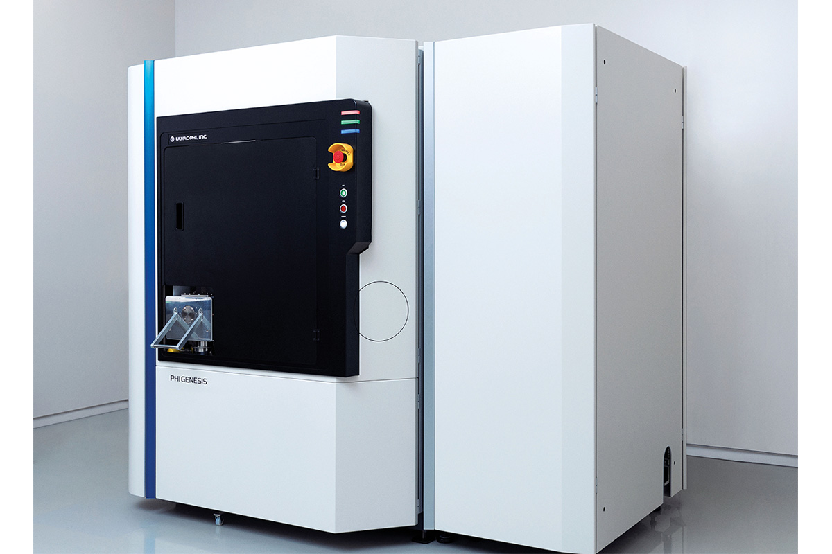
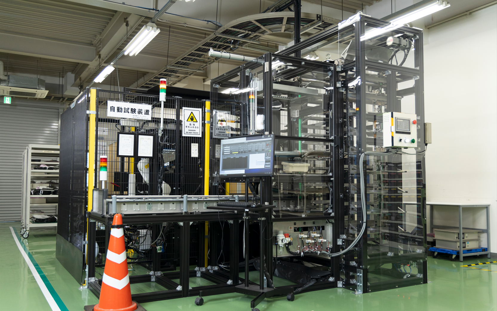
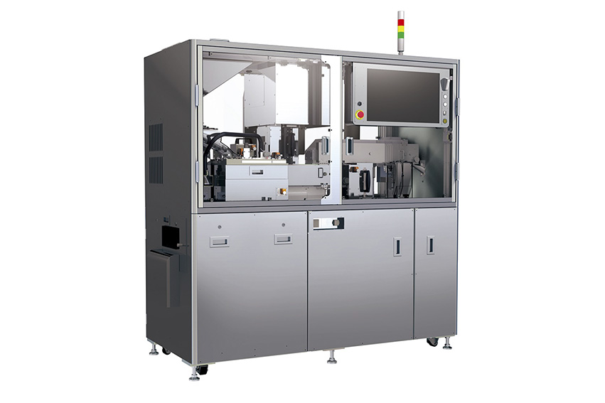
PHI GENESIS: Fully automated multi-tech XPS
The increased adoption of AI in a wide range of industries has been put into overdrive over the past two years. This is also one of the key elements driving the demand for semiconductors since AI systems require powerful semiconductor chips to process huge amounts of data. What do you expect to see from the semiconductor industry in general moving forward and what are some of the key products you’ve developed to adapt to the growing demand in this sector?
We are the only company dealing with the measurement of XPS, SIMS, and Auger. There are various benefits to each of these as well as weaknesses. We understand the pluses and minuses of all of these technologies. Thanks to our profound depth of understanding of these technologies, we are therefore able to recognize the needs of our clients and even the potential possibilities of these technologies. We are able to provide optimal solutions to our clients.
One of your standout products is the PHI GENESIS, an x-ray electron spectroscopy machine that you released in July 2022. Can you introduce us in more detail to the PHI GENESIS machine and how it is superior to other more conventional products in the market?
In terms of the genesis of XPS or X-ray electron spectroscopy, up until that time, we had four different instruments that were in play. According to our customers, they would purchase one or the other depending on their needs, but due to further deepening our research and understanding from the customer’s perspective, we understood that their objective at the time of purchase changes as they continue to utilize the device. Slowly as they use the device, new needs may emerge. We understood that there was a need for many different functions and some of those functions might not be necessarily utilized at first when a client purchases the device.
We are a market-driven company and our objective is to be driven by market research. We have a strong corporate purpose to become a company that is always thinking about what will best serve the customers, not what will sell the most. The PHI GENESIS is really the crystallization of all of our thought processes and technologies into one package that meets customer needs to the fullest.
Manufacturing these types of machines obviously comes with challenges such as finding the right balance between cost efficiency and high precision. How are you able to overcome all of the challenges associated with producing the most efficient and reliable machines for your customers?
What we have been able to provide is our key strength, and that lies in our diversification and our R&D capacity. Our R&D department is not one-dimensional, rather it is multifaceted and we are able to incorporate diverse perspectives during development. This is the result of the synergies across our parent companies. R&D facilities in the US and Japan are not doing the same thing; they have different functionalities. They are able to support one another by sharing the same purpose but coming at the problem from different angles. This not only strengthens the solutions we can provide but it also fortifies the impact that we can have.
During our research, we came across the PHI nanoTOF 3+, a high-precision analysis TRIFT analyzer with a unique, ION beam technology integrated. Could you explain to us what Parallel Imaging MS/MS is?
Ion identification, structural elucidation, and high-resolution imaging within a tandem MS analysis. PHI’s TOF-TOF spectrometer enables the generation of pure, single-molecule spectra from the complex mixture spectrum which greatly simplifies data interpretation and peak identification. Molecular identification and imaging are achieved at the highest sensitivity; therefore, one-of-a-kind samples may be probed repeatedly for the identification of numerous molecular precursors.
What real-world applications and scientific fields will most benefit from the PHI nanoTOF 3+?
Batteries will benefit the most, I think, but then there are also lots of applications within the semiconductor field. The key benefit is not only the 2D imaging but the fact that the device can produce 3D images. It allows users to see the depth of a material which is very important.
Specifically, what this product leads to is quality management and quality control. Users are able to analyze when something is broken or faulty and then troubleshoot.
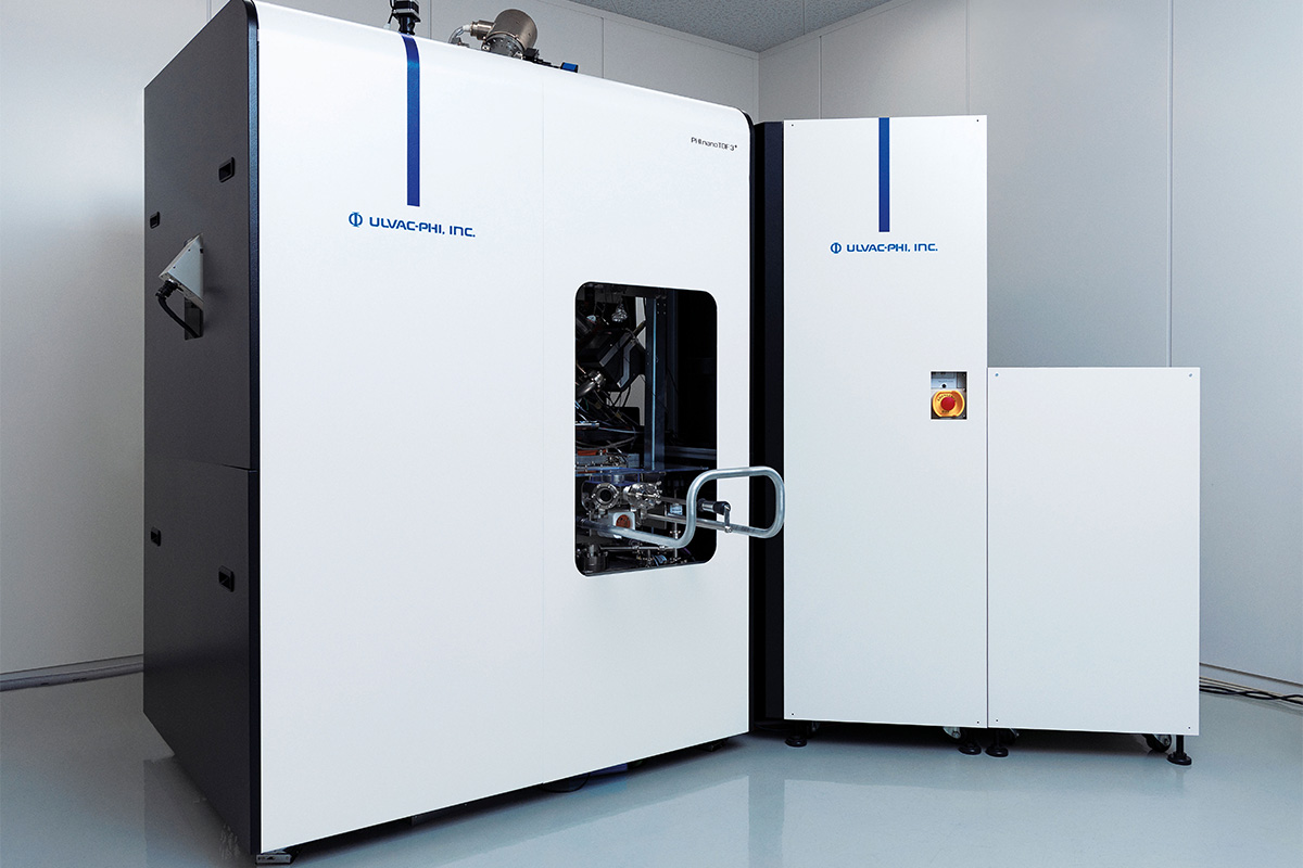
PHI nanoTOF3+: Latest generation of TOF-SIMS
Your company’s presence is felt all around the globe, so moving forward where would you like to expand your presence to next, and what strategies will you employ to do so?
When it comes to China, we established a new company there last year and we feel at this point we have been able to define most of the foundations for developing our business in China. However, when it comes to where we want to place our feet next, that would be in more emerging markets such as Southeast Asia, India, and the Middle East. We’ve actually already started taking the first steps in opening up our efforts in these markets moving forward. Additionally, we are also looking to continue to strengthen our presence in the European market, a key location for cutting-edge innovation.
Imagine that we come back in three years and have this interview all over again. What goals or dreams do you hope to achieve by the time we come back for that new interview?
In terms of our mid-term objectives, they are very clear for the next two to three years. We already have a leading share when it comes to the surface analysis instrument market, but we want to get even bigger than that. We want to be the unquestionable giant, the unquestionable leader of the global market. In this process, we want to blaze open new possibilities for applications of our technology. Towards this end, we are putting huge investments into R&D and therefore are actively seeking R&D partners around the world to grow with us.


0 COMMENTS