Vision/Mission
The "Philosophy" of Meiko Group
Meiko Group practices fair competition in its pursuit of reasonable profits and works for the greater good of society. Meiko Group respects the rights of all people, complies with laws and regulations, honors global rules and their underlying morals, and act as a responsible global company with high ideals that contributes to the creation of a sustainable society through its business activities, both in Japan and other countries around the world. The corporate charter that governs our actions is based on the following nine principles:
Business Description
Meiko provides state-of-the-art products, such as AnyLayer HDI ,which offer free connection among all layers, adapted to the shrinking size of mobile phones and other handheld devices, as well as high heat dissipation PCBs and high electric current PCBs capable of withstanding harsh environments like the inside of car engines and solar power generators.

Meiko possesses state-of-the-art CAD systems capable of designing the optimal wiring for a limited space within a short period of time. Fully applying our production know-how straight from the design stage allows us to make the smooth transition to mass production.

Meiko provides high-reliability, high-precision, and high-quality solder stencils manufactured in state-of-the-art facilities at our production sites in Japan and other countries. From design to application, our metal masks have a proven record in a wide variety of fields, such as mobile devices, automobiles, and consumer devices. In addition, our integrated production and sales system has enabled us to achieve the shortest delivery times in the industry.

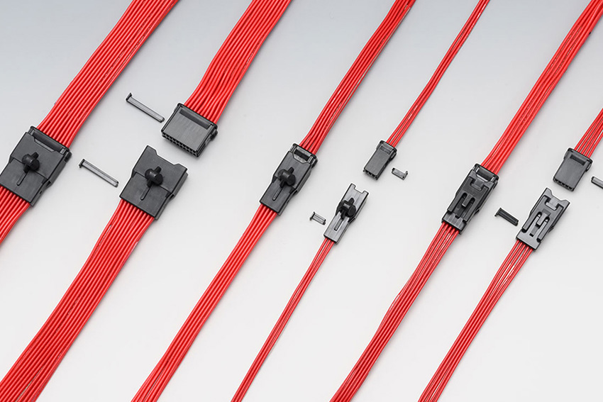
Meiko provides a total solution service to support our customers and help them flexibly adapt to changes in the market. This service integrates the outsourcing of all the processes involved in production, including pattern designing, manufacturing, component procurement, implementation, inspection, and shipment.

When it comes to PCBs composed of numerous components, it is essential to have inspection technology that verifies the position and size of patterns and holes with micron precision. Meiko uses its PCB manufacturing expertise to provide PCB hole inspection systems and electricity checkers.
Meiko’s imaging division developed and is manufacturing the world’s first multivision video magnifying device (processor) and peripherals, such as matrix switchers and converters. These products are widely used both in Japan and other countries.
Background

Products/Services

Markets

Location
Address
5-14-15, Ogami, Ayase, Kanagawa 252-1104, Japan
Tel
+81-0467-76-6001

Yamagata Meiko Electronics Co., Ltd. | Manufacture of PCBs |
Meiko Tech Co., Ltd. | Sales of PCBs |
Meiko Techno Co., Ltd. | Manufacture and sale of electrical machinery and equipment. |
MD Systems Co., Ltd. | CAD Center for designing PCBs |
Meiko Elec. Hong Kong. Co., Ltd. | Sales of PCBs |
Meiko Electronics (Guangzhou Nansha) Co., Ltd. | Manufacture of PCBs |
Meiko Electronics (Wuhan) Co., Ltd. | Manufacture of PCBs |
MDS Circuit Technology, Inc. | CAD Center for designing PCBs |
Meiko Electronics America, Inc. | Sales of PCBs |
Meiko Electronics Europe GmbH | Sales of PCBs |
Meiko Electronics Vietnam Co., Ltd. | Manufacture of PCBs.EMS. |
Meiko Electronics Thang Long Co., Ltd. | Manufacture of PCBs |
Competitive Advantages
43 Years Rich experiences in PCB industry,run by founder of company
W/W Rank 5th In automotive PCB in 2016
W/W Rank 4th In HDI PCB in 2016
20 Years in China Set-up Guang Zhou factory in 1998
Overall Tech Capability Possess of technology for automotive(reliability)& Smart phone(high density)
Excellent Quality Excellent-Quality award & Technical Symposium
W/W Rank 8th In PCB industry in 2016
Eco-Friendly ✓Fukushima Solar Power Plant. ✓Eco-Friendly Organization Approved for GZ factory
Financial Projection